EVAL-AD7706EB Analog Devices Inc, EVAL-AD7706EB Datasheet - Page 2
EVAL-AD7706EB
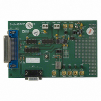
Manufacturer Part Number
EVAL-AD7706EB
Description
BOARD EVAL FOR AD7706
Manufacturer
Analog Devices Inc
Datasheet
1.EVAL-AD7705EB.pdf
(32 pages)
Specifications of EVAL-AD7706EB
Number Of Adc's
1
Number Of Bits
16
Sampling Rate (per Second)
500
Data Interface
Serial
Inputs Per Adc
3 Differential
Input Range
0 ~ 5.25 V
Power (typ) @ Conditions
6.5mW @ 500SPS
Voltage Supply Source
Single
Operating Temperature
-40°C ~ 85°C
Utilized Ic / Part
AD7706
Lead Free Status / RoHS Status
Contains lead / RoHS non-compliant


AD7705/AD7706–SPECIFICATIONS
with V
Parameter
STATIC PERFORMANCE
ANALOG INPUTS/REFERENCE INPUTS
LOGIC INPUTS
No Missing Codes
Output Noise
Integral Nonlinearity
Unipolar Offset Error
Unipolar Offset Drift
Bipolar Zero Error
Bipolar Zero Drift
Positive Full-Scale Error
Full-Scale Drift
Gain Error
Gain Drift
Bipolar Negative Full-Scale Error
Bipolar Negative Full-Scale Drift
Input Common-Mode Rejection (CMR)
Normal-Mode 50 Hz Rejection
Normal-Mode 60 Hz Rejection
Common-Mode 50 Hz Rejection
Common-Mode 60 Hz Rejection
Absolute/Common-Mode REF IN Voltage
Absolute/Common-Mode AIN Voltage
Absolute/Common-Mode AIN Voltage
AIN DC Input Current
AIN Sampling Capacitance
AIN Differential Voltage Range
AIN Input Sampling Rate, f
Reference Input Range
Input Current
All Inputs Except SCLK and MCLK IN
SCLK Only (Schmitt Triggered Input)
SCLK Only (Schmitt Triggered Input)
MCLK IN Only
MCLK IN Only
V
V
REF IN(+) – REF IN(–) Voltage
REF IN(+) – REF IN(–) Voltage
REF IN Input Sampling Rate, f
All Inputs Except MCLK IN
MCLK
V
V
V
V
V
V
V
V
V
V
V
V
DD
DD
DD
INL
INH
T+
T–
T+
T+
T–
T+
INL
INH
INL
INH
Gain = 1
Gain = 2
Gain = 4
Gain = 8v128
Gain = 1
Gain = 2
Gain = 4
Gain = 8v128
= 5 V; REF IN(–) = GND; MCLK IN = 2.4576 MHz unless otherwise noted. All specifications T
, Input Low Voltage
– V
– V
, Input Low Voltage
, Input Low Voltage
= 5 V
= 3 V
, Input High Voltage
, Input High Voltage
, Input High Voltage
4, 8
T–
T–
7
4, 6
4
2
4
2
5
2
S
2
2
10
4
2
2
2
S
2, 9
2, 9
2
2
B Version
16
See Tables I and III
See Note 3
0.5
See Note 3
0.5
0.1
See Note 3
0.5
See Note 3
0.5
1
0.6
96
105
110
130
105
110
120
130
98
98
150
150
GND to V
GND – 30 mV
V
GND + 50 mV
V
1
10
0 to +V
GAIN
f
1/1.75
1/3.5
f
0.8
0.4
2.0
1.4/3
0.8/1.4
0.4/0.8
1/2.5
0.4/1.1
0.375/0.8
0.8
3.5
0.4
2.5
CLKIN
CLKIN
0.003
0.003
V
1
10
DD
DD
REF
+ 30 mV
– 1.5 V
/8
/64
/GAIN
REF
f
CLKIN
DD
1
/GAIN
/64
11
Units
Bits min
% of FSR max
ppm of FSR/ C typ
% of FSR typ
dB typ
dB typ
dB typ
dB typ
dB typ
dB typ
dB typ
dB typ
dB typ
dB typ
dB typ
dB typ
V min to V max
V min
V max
V min
V max
nA max
pF max
nom
nom
V min/max
V min/max
V max
V max
V min
V min/V max
V min/V max
V min/V max
V min/V max
V min/V max
V min/V max
V max
V min
V max
V min
V/ C typ
V/ C typ
V/ C typ
V/ C typ
V/ C typ
V/ C typ
A max
A max
–2–
(V
DD
= +3 V or 5 V, REF IN(+) = +1.225 V with V
Conditions/Comments
Guaranteed by Design. Filter Notch < 60 Hz
Depends on Filter Cutoffs and Selected Gain
Filter Notch < 60 Hz. Typically 0.0003%
For Gains 1, 2 and 4
For Gains 8, 16, 32, 64 and 128
Typically 0.001%
For Gains of 1 to 4
For Gains of 8 to 128
Specifications for AIN and REF IN Unless Noted
For Filter Notches of 25 Hz, 50 Hz, 0.02
For Filter Notches of 20 Hz, 60 Hz, 0.02
For Filter Notches of 25 Hz, 50 Hz, 0.02
For Filter Notches of 20 Hz, 60 Hz, 0.02
BUF Bit of Setup Register = 0
BUF Bit of Setup Register = 1
Unipolar Input Range (B/U Bit of Setup Register = 1)
Bipolar Input Range (B/U Bit of Setup Register = 0)
For Gains of 1 to 4
For Gains of 8 to 128
V
Performance
V
Performance
Typically 20 nA
Typically 2 A
V
V
V
V
V
V
V
DD
DD
DD
DD
DD
DD
DD
DD
DD
= 2.7 V to 3.3 V. V
= 4.75 V to 5.25 V. V
= 5 V
= 3 V
= 3 V and 5 V
= 5 V NOMINAL
= 3 V NOMINAL
= 5 V NOMINAL
= 3 V NOMINAL
MIN
to T
MAX
unless otherwise noted.)
REF
REF
= 1.225
= 2.5
DD
1% for Specified
1% for Specified
= 3 V and +2.5 V
f
f
f
f
NOTCH
NOTCH
NOTCH
NOTCH
REV. A
Related parts for EVAL-AD7706EB
Image
Part Number
Description
Manufacturer
Datasheet
Request
R

Part Number:
Description:
ENERCHIP CC EVAL KIT
Manufacturer:
Cymbet Corporation
Datasheet:

Part Number:
Description:
BOARD EVAL FOR AD976
Manufacturer:
Analog Devices Inc
Datasheet:

Part Number:
Description:
BOARD EVAL FOR ADXL345
Manufacturer:
Analog Devices Inc
Datasheet:

Part Number:
Description:
ENERCHIP CC SEH EVAL KIT
Manufacturer:
Cymbet Corporation
Datasheet:

Part Number:
Description:
ENERCHIP EP ENERGY HARVEST EVAL
Manufacturer:
Cymbet Corporation
Datasheet:

Part Number:
Description:
EVAL BOARD FOR TW6864-LB2-GR
Manufacturer:
Intersil
Datasheet:
Part Number:
Description:
EVAL BOARD FOR TW8816-LB3-GR
Manufacturer:
Intersil
Datasheet:
Part Number:
Description:
EVAL BOARD FOR TW8817-TA3-GRS
Manufacturer:
Intersil
Datasheet:

Part Number:
Description:
EVALUATION MODULE FOR ADUM4160
Manufacturer:
Analog Devices Inc
Datasheet:

Part Number:
Description:
BOARD EVALUATION ADCMP581BCP
Manufacturer:
Analog Devices Inc
Datasheet:
Part Number:
Description:
BOARD EVALUATION ADM1041
Manufacturer:
Analog Devices Inc
Datasheet:

Part Number:
Description:
EVAL BOARD FOR STM32F107VCT
Manufacturer:
STMicroelectronics
Datasheet:
Part Number:
Description:
BOARD EVAL FOR AD1954
Manufacturer:
Analog Devices Inc
Datasheet:
Part Number:
Description:
BOARD EVAL FOR AD1955
Manufacturer:
Analog Devices Inc
Datasheet:

Part Number:
Description:
BOARD EVAL FOR AD7655
Manufacturer:
Analog Devices Inc
Datasheet: