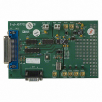
EVAL-AD7706EB Analog Devices Inc, EVAL-AD7706EB Datasheet - Page 17
EVAL-AD7706EB
Manufacturer Part Number
EVAL-AD7706EB
Description
BOARD EVAL FOR AD7706
Manufacturer
Analog Devices Inc
Datasheet
1.EVAL-AD7705EB.pdf
(32 pages)
Specifications of EVAL-AD7706EB
Number Of Adc's
1
Number Of Bits
16
Sampling Rate (per Second)
500
Data Interface
Serial
Inputs Per Adc
3 Differential
Input Range
0 ~ 5.25 V
Power (typ) @ Conditions
6.5mW @ 500SPS
Voltage Supply Source
Single
Operating Temperature
-40°C ~ 85°C
Utilized Ic / Part
AD7706
Lead Free Status / RoHS Status
Contains lead / RoHS non-compliant


Bipolar or unipolar options are chosen by programming the B/U
bit of the Setup Register. This programs the channel for either
unipolar or bipolar operation. Programming the channel for
either unipolar or bipolar operation does not change any of the
input signal conditioning, it simply changes the data output
coding and the points on the transfer function where calibra-
tions occur.
REFERENCE INPUT
The AD7705/AD7706’s reference inputs, REF IN(+) and
REF IN(–), provide a differential reference input capability.
The common-mode range for these differential inputs is from
GND to V
REF IN(–)), for specified operation, is +2.5 V for the AD7705/
AD7706 operated with a V
AD7705/AD7706 operated with a V
tional with V
formance as the output noise will, in terms of LSB size, be larger.
REF IN(+) must always be greater than REF IN(–) for correct
operation of the AD7705/AD7706.
Both reference inputs provide a high impedance, dynamic load
similar to the analog inputs in unbuffered mode. The maximum
dc input leakage current is 1 nA over temperature, and source
resistance may result in gain errors on the part. In this case, the
sampling switch resistance is 5 k typ and the reference capaci-
tor (C
inputs is f
and 2, C
32, it is 4.25 pF, for a gain of 64, it is 3.625 pF and for a gain of
128, it is 3.3125 pF.
The output noise performance outlined in Tables I through IV
is for an analog input of 0 V, which effectively removes the
effect of noise on the reference. To obtain the same noise per-
formance as shown in the noise tables over the full input range
requires a low noise reference source for the AD7705/AD7706.
If the reference noise in the bandwidth of interest is excessive, it
will degrade the performance of the AD7705/AD7706. In appli-
cations where the excitation voltage for the bridge transducer on
the analog input also derives the reference voltage for the part,
the effect of the noise in the excitation voltage will be removed
as the application is ratiometric. Recommended reference volt-
age sources for the AD7705 with a V
AD780, REF43 and REF192, while the recommended reference
sources for the AD7705 operated with a V
AD589 and AD1580. It is generally recommended to decouple
the output of these references in order to further reduce the
noise level.
DIGITAL FILTERING
The AD7705/AD7706 contains an on-chip low-pass digital filter
which processes the output of the part’s sigma-delta modulator.
Therefore, the part not only provides the analog-to-digital con-
version function but also provides a level of filtering. There are a
number of system differences when the filtering function is
provided in the digital domain rather than the analog domain
and the user should be aware of these.
First, since digital filtering occurs after the A-to-D conversion
process, it can remove noise injected during the conversion
process. Analog filtering cannot do this. Also, the digital filter
can be made programmable far more readily than an analog
filter. Depending on the digital filter design, this gives the user
REV. A
REF
REF
) varies with gain. The sample rate on the reference
CLKIN
DD
is 8 pF; for a gain of 16, it is 5.5 pF, for a gain of
. The nominal reference voltage, V
REF
/64 and does not vary with gain. For gains of 1
voltages down to 1 V, but with degraded per-
DD
of 5 V and +1.225 V for the
DD
DD
of 3 V. The part is func-
of 5 V include the
DD
of 3 V include the
REF
(REF IN(+) –
–17–
the capability of programming cutoff frequency and output
update rate.
On the other hand, analog filtering can remove noise superim-
posed on the analog signal before it reaches the ADC. Digital
filtering cannot do this and noise peaks riding on signals near
full scale have the potential to saturate the analog modulator
and digital filter, even though the average value of the signal is
within limits. To alleviate this problem, the AD7705/AD7706
has overrange headroom built into the sigma-delta modulator
and digital filter, which allows overrange excursions of 5%
above the analog input range. If noise signals are larger than
this, consideration should be given to analog input filtering, or
to reducing the input channel voltage so that its full-scale is half
that of the analog input channel full-scale. This will provide an
overrange capability greater than 100% at the expense of reduc-
ing the dynamic range by 1 bit (50%).
In addition, the digital filter does not provide any rejection at
integer multiples of the digital filter’s sample frequency. How-
ever, the input sampling on the part provides attenuation at
multiples of the digital filter’s sampling frequency so that the
unattenuated bands actually occur around multiples of the
sampling frequency f
unattenuated bands occur at n f
these frequencies, there are frequency bands, f
the cutoff frequency of the digital filter) at either side where
noise passes unattenuated to the output.
Filter Characteristics
The AD7705/AD7706’s digital filter is a low-pass filter with a
(sinx/x)
this filter is described in the z-domain by:
and in the frequency domain by:
where N is the ratio of the modulator rate to the output rate.
Phase Response:
Figure 4 shows the filter frequency response for a cutoff fre-
quency of 15.72 Hz, which corresponds to a first filter notch
frequency of 60 Hz. The plot is shown from dc to 390 Hz. This
response is repeated at either side of the digital filter’s sample
frequency and at either side of multiples of the filter’s sample
frequency.
The response of the filter is similar to that of an averaging filter,
but with a sharper roll-off. The output rate for the digital filter
corresponds with the positioning of the first notch of the filter’s
frequency response. Thus, for the plot of Figure 12 where the
output rate is 60 Hz, the first notch of the filter is at 60 Hz. The
notches of this (sinx/x)
first notch. The filter provides attenuation of better than 100 dB
at these notches.
3
response (also called sinc
H( f )
H
S
H(z)
3
N
(as defined in Table XV). Thus the
1
–3 (N – 2) f /f
filter are repeated at multiples of the
SIN(N
N
1
SIN(
S
1 Z
3
1 Z
). The transfer function for
AD7705/AD7706
(where n = 1, 2, 3 . . .). At
–N
–1
f /f
S
3
f /f
S
Rad
)
S
)
3 dB
3
wide f
3 dB
is
Related parts for EVAL-AD7706EB
Image
Part Number
Description
Manufacturer
Datasheet
Request
R

Part Number:
Description:
ENERCHIP CC EVAL KIT
Manufacturer:
Cymbet Corporation
Datasheet:

Part Number:
Description:
BOARD EVAL FOR AD976
Manufacturer:
Analog Devices Inc
Datasheet:

Part Number:
Description:
BOARD EVAL FOR ADXL345
Manufacturer:
Analog Devices Inc
Datasheet:

Part Number:
Description:
ENERCHIP CC SEH EVAL KIT
Manufacturer:
Cymbet Corporation
Datasheet:

Part Number:
Description:
ENERCHIP EP ENERGY HARVEST EVAL
Manufacturer:
Cymbet Corporation
Datasheet:

Part Number:
Description:
EVAL BOARD FOR TW6864-LB2-GR
Manufacturer:
Intersil
Datasheet:
Part Number:
Description:
EVAL BOARD FOR TW8816-LB3-GR
Manufacturer:
Intersil
Datasheet:
Part Number:
Description:
EVAL BOARD FOR TW8817-TA3-GRS
Manufacturer:
Intersil
Datasheet:

Part Number:
Description:
EVALUATION MODULE FOR ADUM4160
Manufacturer:
Analog Devices Inc
Datasheet:

Part Number:
Description:
BOARD EVALUATION ADCMP581BCP
Manufacturer:
Analog Devices Inc
Datasheet:
Part Number:
Description:
BOARD EVALUATION ADM1041
Manufacturer:
Analog Devices Inc
Datasheet:

Part Number:
Description:
EVAL BOARD FOR STM32F107VCT
Manufacturer:
STMicroelectronics
Datasheet:
Part Number:
Description:
BOARD EVAL FOR AD1954
Manufacturer:
Analog Devices Inc
Datasheet:
Part Number:
Description:
BOARD EVAL FOR AD1955
Manufacturer:
Analog Devices Inc
Datasheet:

Part Number:
Description:
BOARD EVAL FOR AD7655
Manufacturer:
Analog Devices Inc
Datasheet: