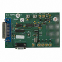
EVAL-AD7706EB Analog Devices Inc, EVAL-AD7706EB Datasheet - Page 24
EVAL-AD7706EB
Manufacturer Part Number
EVAL-AD7706EB
Description
BOARD EVAL FOR AD7706
Manufacturer
Analog Devices Inc
Datasheet
1.EVAL-AD7705EB.pdf
(32 pages)
Specifications of EVAL-AD7706EB
Number Of Adc's
1
Number Of Bits
16
Sampling Rate (per Second)
500
Data Interface
Serial
Inputs Per Adc
3 Differential
Input Range
0 ~ 5.25 V
Power (typ) @ Conditions
6.5mW @ 500SPS
Voltage Supply Source
Single
Operating Temperature
-40°C ~ 85°C
Utilized Ic / Part
AD7706
Lead Free Status / RoHS Status
Contains lead / RoHS non-compliant


AD7705/AD7706
Figures 16 and 17 show timing diagrams for interfacing to the
AD7705/AD7706 with CS used to decode the part. Figure 16 is
for a read operation from the AD7705/AD7706’s output shift
register while Figure 17 shows a write operation to the input
shift register. It is possible to read the same data twice from the
output register even though the DRDY line returns high after
the first read operation. Care must be taken, however, to ensure
that the read operations have been completed before the next
output update is about to take place.
The AD7705/AD7706 serial interface can operate in three-wire
mode by tying the CS input low. In this case, the SCLK, DIN
and DOUT lines are used to communicate with the AD7705/
AD7706 and the status of DRDY can be obtained by interrogat-
ing the MSB of the Communications Register. This scheme is
suitable for interfacing to microcontrollers. If CS is required as a
decoding signal, it can be generated from a port bit. For
microcontroller interfaces, it is recommended that the SCLK
idles high between data transfers.
The AD7705/AD7706 can also be operated with CS used as a
frame synchronization signal. This scheme is suitable for DSP
interfaces. In this case, the first bit (MSB) is effectively clocked
out by CS since CS would normally occur after the falling edge
of SCLK in DSPs. The SCLK can continue to run between
data transfers provided the timing numbers are obeyed.
DRDY
DOUT
SCLK
SCLK
DIN
CS
CS
t
5
t
12
t
3
t
t
11
4
MSB
MSB
Figure 17. Write Cycle Timing Diagram
Figure 16. Read Cycle Timing Diagram
t
13
t
t
14
6
t
t
15
7
–24–
The serial interface can be reset by exercising the RESET input
on the part. It can also be reset by writing a series of 1s on the
DIN input. If a Logic 1 is written to the AD7705/AD7706 DIN
line for at least 32 serial clock cycles the serial interface is reset.
This ensures that in three-wire systems, if the interface gets lost
either via a software error or by some glitch in the system, it can
be reset back to a known state. This state returns the interface
to where the AD7705/AD7706 is expecting a write operation to
its Communications Register. This operation in itself does not
reset the contents of any registers but since the interface was
lost, the information written to any of the registers is unknown
and it is advisable to set up all registers again.
Some microprocessor or microcontroller serial interfaces have a
single serial data line. In this case, it is possible to connect the
AD7705/AD7706’s DATA OUT and DATA IN lines together
and connect them to the single data line of the processor. A
10 k pull-up resistor should be used on this single data line. In
this case, if the interface gets lost, because the read and write
operations share the same line the procedure to reset it back to a
known state is somewhat different than previously described. It
requires a read operation of 24 serial clocks followed by a write
operation where a Logic 1 is written for at least 32 serial clock
cycles to ensure that the serial interface is back into a known
state.
LSB
LSB
t
10
t
9
t
t
8
16
REV. A
Related parts for EVAL-AD7706EB
Image
Part Number
Description
Manufacturer
Datasheet
Request
R

Part Number:
Description:
ENERCHIP CC EVAL KIT
Manufacturer:
Cymbet Corporation
Datasheet:

Part Number:
Description:
BOARD EVAL FOR AD976
Manufacturer:
Analog Devices Inc
Datasheet:

Part Number:
Description:
BOARD EVAL FOR ADXL345
Manufacturer:
Analog Devices Inc
Datasheet:

Part Number:
Description:
ENERCHIP CC SEH EVAL KIT
Manufacturer:
Cymbet Corporation
Datasheet:

Part Number:
Description:
ENERCHIP EP ENERGY HARVEST EVAL
Manufacturer:
Cymbet Corporation
Datasheet:

Part Number:
Description:
EVAL BOARD FOR TW6864-LB2-GR
Manufacturer:
Intersil
Datasheet:
Part Number:
Description:
EVAL BOARD FOR TW8816-LB3-GR
Manufacturer:
Intersil
Datasheet:
Part Number:
Description:
EVAL BOARD FOR TW8817-TA3-GRS
Manufacturer:
Intersil
Datasheet:

Part Number:
Description:
EVALUATION MODULE FOR ADUM4160
Manufacturer:
Analog Devices Inc
Datasheet:

Part Number:
Description:
BOARD EVALUATION ADCMP581BCP
Manufacturer:
Analog Devices Inc
Datasheet:
Part Number:
Description:
BOARD EVALUATION ADM1041
Manufacturer:
Analog Devices Inc
Datasheet:

Part Number:
Description:
EVAL BOARD FOR STM32F107VCT
Manufacturer:
STMicroelectronics
Datasheet:
Part Number:
Description:
BOARD EVAL FOR AD1954
Manufacturer:
Analog Devices Inc
Datasheet:
Part Number:
Description:
BOARD EVAL FOR AD1955
Manufacturer:
Analog Devices Inc
Datasheet:

Part Number:
Description:
BOARD EVAL FOR AD7655
Manufacturer:
Analog Devices Inc
Datasheet: