EVAL-AD7706EB Analog Devices Inc, EVAL-AD7706EB Datasheet - Page 19
EVAL-AD7706EB
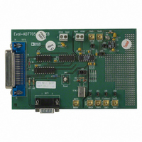
Manufacturer Part Number
EVAL-AD7706EB
Description
BOARD EVAL FOR AD7706
Manufacturer
Analog Devices Inc
Datasheet
1.EVAL-AD7705EB.pdf
(32 pages)
Specifications of EVAL-AD7706EB
Number Of Adc's
1
Number Of Bits
16
Sampling Rate (per Second)
500
Data Interface
Serial
Inputs Per Adc
3 Differential
Input Range
0 ~ 5.25 V
Power (typ) @ Conditions
6.5mW @ 500SPS
Voltage Supply Source
Single
Operating Temperature
-40°C ~ 85°C
Utilized Ic / Part
AD7706
Lead Free Status / RoHS Status
Contains lead / RoHS non-compliant


Self-Calibration
A self-calibration is initiated on the AD7705/AD7706 by writing
the appropriate values (0, 1) to the MD1 and MD0 bits of
the Setup Register. In the self-calibration mode with a unipo-
lar input range, the zero scale point used in determining the
calibration coefficients is with the inputs of the differential
pair internally shorted on the part (i.e., AIN(+) = AIN(–) =
Internal Bias Voltage in the case of the AD7705 and AIN =
COMMON = Internal Bias voltage on the AD7706). The PGA
is set for the selected gain (as per G1 and G0 bits in the Com-
munications Register) for this zero-scale calibration conversion.
The full-scale calibration conversion is performed at the selected
gain on an internally-generated voltage of V
The duration time for the calibration is 6 1/Output Rate. This
is made up of 3
and 3
the MD1 and MD0 bits in the Setup Register return to 0, 0.
This gives the earliest indication that the calibration sequence is
complete. The DRDY line goes high when calibration is initi-
ated and does not return low until there is a valid new word in
the data register. The duration time from the calibration com-
mand being issued to DRDY going low is 9
This is made up of 3 1/Output Rate for the zero-scale calibra-
tion, 3 1/Output Rate for the full-scale calibration, 3 1/Output
Rate for a conversion on the analog input and some overhead to
correctly set up the coefficients. If DRDY is low before (or goes
low during) the calibration command write to the Setup Regis-
ter, it may take up to one modulator cycle (MCLK IN/128)
before DRDY goes high to indicate that calibration is in progress.
Therefore, DRDY should be ignored for up to one modulator
cycle after the last bit is written to the Setup Register in the
calibration command.
For bipolar input ranges in the self-calibrating mode, the se-
quence is very similar to that just outlined. In this case, the two
points are exactly the same as above but, since the part is config-
ured for bipolar operation, the shorted inputs point is actually
midscale of the transfer function.
System Calibration
System calibration allows the AD7705/AD7706 to compensate
for system gain and offset errors as well as its own internal er-
rors. System calibration performs the same slope factor calcula-
tions as self-calibration, but uses voltage values presented by
the system to the AIN inputs for the zero- and full-scale points.
Full system calibration requires a two-step process, a ZS System
Calibration followed by an FS System Calibration.
For a full system calibration, the zero-scale point must be pre-
sented to the converter first. It must be applied to the converter
before the calibration step is initiated and remain stable until the
step is complete. Once the system zero-scale voltage has been
set up, a ZS System Calibration is then initiated by writing the
appropriate values (1, 0) to the MD1 and MD0 bits of the
Setup Register. The zero-scale system calibration is performed
at the selected gain. The duration of the calibration is 3 1/Output
Rate. At this time, the MD1 and MD0 bits in the Setup Register
return to 0, 0. This gives the earliest indication that the calibra-
tion sequence is complete. The DRDY line goes high when
calibration is initiated and does not return low until there is a
valid new word in the data register. The duration time from
the calibration command being issued to DRDY going low is
4
REV. A
1/Output Rate as the part performs a normal conversion on
1/Output Rate for the full-scale calibration. At this time
1/Output Rate for the zero-scale calibration
REF
1/Output Rate.
/Selected Gain.
–19–
the AIN voltage before DRDY goes low. If DRDY is low before
(or goes low during) the calibration command write to the Setup
Register, it may take up to one modulator cycle (MCLK IN/128)
before DRDY goes high to indicate that calibration is in progress.
Therefore, DRDY should be ignored for up to one modulator
cycle after the last bit is written to the Setup Register in the
calibration command.
After the zero-scale point is calibrated, the full-scale point is
applied to AIN and the second step of the calibration process is
initiated by again writing the appropriate values (1, 1) to MD1
and MD0. Again, the full-scale voltage must be set up before
the calibration is initiated and it must remain stable throughout
the calibration step. The full-scale system calibration is per-
formed at the selected gain. The duration of the calibration is
3
Setup Register return to 0, 0. This gives the earliest indication
that the calibration sequence is complete. The DRDY line goes
high when calibration is initiated and does not return low until
there is a valid new word in the data register. The duration time
from the calibration command being issued to DRDY going low
is 4
on the AIN voltage before DRDY goes low. If DRDY is low
before (or goes low during) the calibration command write to
the Setup Register, it may take up to one modulator cycle
(MCLK IN/128) before DRDY goes high to indicate that cali-
bration is in progress. Therefore, DRDY should be ignored for
up to one modulator cycle after the last bit is written to the
Setup Register in the calibration command.
In the unipolar mode, the system calibration is performed be-
tween the two endpoints of the transfer function; in the bipolar
mode, it is performed between midscale (zero differential volt-
age) and positive full-scale.
The fact that the system calibration is a two-step calibration
offers another feature. After the sequence of a full system cali-
bration has been completed, additional offset or gain calibra-
tions can be performed by themselves to adjust the system zero
reference point or the system gain. Calibrating one of the pa-
rameters, either system offset or system gain, will not affect the
other parameter.
System calibration can also be used to remove any errors from
source impedances on the analog input when the part is used in
unbuffered mode. A simple R, C antialiasing filter on the front
end may introduce a gain error on the analog input voltage, but
the system calibration can be used to remove this error.
Span and Offset Limits
Whenever a system calibration mode is used, there are limits on
the amount of offset and span which can be accommodated.
The overriding requirement in determining the amount of offset
and gain that can be accommodated by the part is the require-
ment that the positive full-scale calibration limit is < 1.05
V
nominal range. The built-in headroom in the AD7705/AD7706’s
analog modulator ensures that the part will still operate cor-
rectly with a positive full-scale voltage that is 5% beyond the
nominal.
The range of input span in both the unipolar and bipolar modes
has a minimum value of 0.8 V
value of 2.1 V
difference between the bottom of the AD7705/AD7706’s input
REF
1/Output Rate. At this time, the MD1 and MD0 bits in the
/GAIN. This allows the input range to go 5% above the
1/Output Rate as the part performs a normal conversion
REF
/GAIN. However, the span (which is the
REF
AD7705/AD7706
/GAIN and a maximum
Related parts for EVAL-AD7706EB
Image
Part Number
Description
Manufacturer
Datasheet
Request
R

Part Number:
Description:
ENERCHIP CC EVAL KIT
Manufacturer:
Cymbet Corporation
Datasheet:

Part Number:
Description:
BOARD EVAL FOR AD976
Manufacturer:
Analog Devices Inc
Datasheet:

Part Number:
Description:
BOARD EVAL FOR ADXL345
Manufacturer:
Analog Devices Inc
Datasheet:

Part Number:
Description:
ENERCHIP CC SEH EVAL KIT
Manufacturer:
Cymbet Corporation
Datasheet:

Part Number:
Description:
ENERCHIP EP ENERGY HARVEST EVAL
Manufacturer:
Cymbet Corporation
Datasheet:

Part Number:
Description:
EVAL BOARD FOR TW6864-LB2-GR
Manufacturer:
Intersil
Datasheet:
Part Number:
Description:
EVAL BOARD FOR TW8816-LB3-GR
Manufacturer:
Intersil
Datasheet:
Part Number:
Description:
EVAL BOARD FOR TW8817-TA3-GRS
Manufacturer:
Intersil
Datasheet:

Part Number:
Description:
EVALUATION MODULE FOR ADUM4160
Manufacturer:
Analog Devices Inc
Datasheet:

Part Number:
Description:
BOARD EVALUATION ADCMP581BCP
Manufacturer:
Analog Devices Inc
Datasheet:
Part Number:
Description:
BOARD EVALUATION ADM1041
Manufacturer:
Analog Devices Inc
Datasheet:

Part Number:
Description:
EVAL BOARD FOR STM32F107VCT
Manufacturer:
STMicroelectronics
Datasheet:
Part Number:
Description:
BOARD EVAL FOR AD1954
Manufacturer:
Analog Devices Inc
Datasheet:
Part Number:
Description:
BOARD EVAL FOR AD1955
Manufacturer:
Analog Devices Inc
Datasheet:

Part Number:
Description:
BOARD EVAL FOR AD7655
Manufacturer:
Analog Devices Inc
Datasheet: