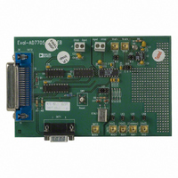
EVAL-AD7706EB Analog Devices Inc, EVAL-AD7706EB Datasheet - Page 27

EVAL-AD7706EB
Manufacturer Part Number
EVAL-AD7706EB
Description
BOARD EVAL FOR AD7706
Manufacturer
Analog Devices Inc
Datasheet
1.EVAL-AD7705EB.pdf
(32 pages)
Specifications of EVAL-AD7706EB
Number Of Adc's
1
Number Of Bits
16
Sampling Rate (per Second)
500
Data Interface
Serial
Inputs Per Adc
3 Differential
Input Range
0 ~ 5.25 V
Power (typ) @ Conditions
6.5mW @ 500SPS
Voltage Supply Source
Single
Operating Temperature
-40°C ~ 85°C
Utilized Ic / Part
AD7706
Lead Free Status / RoHS Status
Contains lead / RoHS non-compliant
interface lines to three, is to monitor the DRDY output line
from the AD7705/AD7706. The monitoring of the DRDY line
can be done in two ways. First, DRDY can be connected to one
of the 8XC51’s port bits (such as P1.0) which is configured as
an input. This port bit is then polled to determine the status of
DRDY. The second scheme is to use an interrupt-driven system,
in which case the DRDY output is connected to the INT1 input
of the 8XC51. For interfaces that require control of the CS
input on the AD7705/AD7706, one of the port bits of the
8XC51 (such as P1.1), which is configured as an output, can be
used to drive the CS input. The 8XC51 is configured in its
Mode 0 serial interface mode. Its serial interface contains a
single data line. As a result, the DATA OUT and DATA IN
pins of the AD7705/AD7706 should be connected together with
a 10 k pull-up resistor. The serial clock on the 8XC51 idles
high between data transfers. The 8XC51 outputs the LSB first
in a write operation, while the AD7705/AD7706 expects the
MSB first so the data to be transmitted has to be rearranged
before being written to the output serial register. Similarly,
the AD7705/AD7706 outputs the MSB first during a read op-
eration while the 8XC51 expects the LSB first. Therefore, the
data read into the serial buffer needs to be rearranged before the
correct data word from the AD7705/AD7706 is available in the
accumulator.
REV. A
Figure 21. AD7705/AD7706 to ADSP-2103/ADSP-2105
Interface
ADSP-2103/
ADSP-2105
SCLK
RFS
TFS
DR
DT
V
DD
RESET
CS
DATA OUT
DATA IN
SCLK
AD7705/AD7706
–27–
AD7705/AD7706 to ADSP-2103/ADSP-2105 Interface
Figure 21 shows an interface between the AD7705/AD7706 and
the ADSP-2103/ADSP-2105 DSP processor. In the interface
shown, the DRDY bit of the Communications Register is again
monitored to determine when the Data Register is updated. The
alternative scheme is to use an interrupt-driven system, in which
case the DRDY output is connected to the IRQ2 input of the
ADSP-2103/ADSP-2105. The serial interface of the ADSP-
2103/ADSP-2105 is set up for alternate framing mode. The
RFS and TFS pins of the ADSP-2103/ADSP-2105 are config-
ured as active low outputs and the ADSP-2103/ADSP-2105
serial clock line, SCLK, is also configured as an output. The CS
for the AD7705/AD7706 is active when either the RFS or TFS
outputs from the ADSP-2103/ADSP-2105 are active. The serial
clock rate on the ADSP-2103/ADSP-2105 should be limited to
3 MHz to ensure correct operation with the AD7705/AD7706.
CODE FOR SETTING UP THE AD7705/AD7706
Table XVII gives a set of read and write routines in C code for
interfacing the 68HC11 microcontroller to the AD7705. The
sample program sets up the various registers on the AD7705
and reads 1000 samples from the part into the 68HC11. The
setup conditions on the part are exactly the same as those out-
lined for the flowchart of Figure 18. In the example code given
here, the DRDY output is polled to determine if a new valid
word is available in the data register. The very same sequence is
applicable for the AD7706.
The sequence of the events in this program are as follows:
1. Write to the Communications Register, selecting channel one
2. Write to Clock Register setting the CLK DIV bit which
3. Write to Communication Register selecting Channel 1 as the
4. Write to the Setup Register, setting the gain to 1, setting
5. Poll the DRDY output.
6. Read the data from the Data Register.
7. Loop around doing Steps 5 and 6 until the specified number
as the active channel and setting the next operation to be a
write to the clock register.
divides the external clock internally by two. This assumes
that the external crystal is 4.9512 MHz. The update rate is
selected to be 50 Hz.
active channel and setting the next operation to be a write to
the Setup Register.
bipolar mode, buffer off, clearing the filter synchronization
and initiating a self-calibration.
of samples have been taken from the selected channel.
AD7705/AD7706


