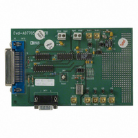
EVAL-AD7706EB Analog Devices Inc, EVAL-AD7706EB Datasheet - Page 4
EVAL-AD7706EB
Manufacturer Part Number
EVAL-AD7706EB
Description
BOARD EVAL FOR AD7706
Manufacturer
Analog Devices Inc
Datasheet
1.EVAL-AD7705EB.pdf
(32 pages)
Specifications of EVAL-AD7706EB
Number Of Adc's
1
Number Of Bits
16
Sampling Rate (per Second)
500
Data Interface
Serial
Inputs Per Adc
3 Differential
Input Range
0 ~ 5.25 V
Power (typ) @ Conditions
6.5mW @ 500SPS
Voltage Supply Source
Single
Operating Temperature
-40°C ~ 85°C
Utilized Ic / Part
AD7706
Lead Free Status / RoHS Status
Contains lead / RoHS non-compliant


AD7705/AD7706
TIMING CHARACTERISTICS
Parameter
f
t
t
t
t
Read Operation
Write Operation
NOTES
1
2
3
4
5
6
7
See Figures 16 and 17.
f
The AD7705/AD7706 is production tested with f
These numbers are measured with the load circuit of Figure 1 and defined as the time required for the output to cross the V
These numbers are derived from the measured time taken by the data output to change 0.5 V when loaded with the circuit of Figure 1. The measured number is
DRDY returns high after the first read from the device after an output update. The same data can be read again, if required, while DRDY is high, although care
CLKIN
CLKIN LO
CLKIN HI
1
2
Sample tested at +25 C to ensure compliance. All input signals are specified with tr = tf = 5 ns (10% to 90% of V
can draw higher current than specified and possibly become uncalibrated.
then extrapolated back to remove effects of charging or discharging the 50 pF capacitor. This means that the times quoted in the timing characteristics are the
true bus relinquish times of the part and as such are independent of external bus loading capacitances.
should be taken that subsequent reads do not occur close to the next output update.
CLKIN
t
t
t
t
t
t
t
t
t
t
t
t
t
t
3
4
5
6
7
8
9
10
11
12
13
14
15
16
5
6
Duty Cycle range is 45% to 55%. f
3, 4
Limit at T
(B Version)
400
2.5
0.4
0.4
500
100
0
120
0
80
100
100
100
0
10
60
100
100
120
30
20
100
100
0
t
t
t
CLKIN
CLKIN
CLKIN
Figure 1. Load Circuit for Access Time and Bus Relinquish Time
CLKIN
MIN
, T
must be supplied whenever the AD7705/AD7706 is not in Standby mode. If no clock is present in this case, the device
CLKIN
1, 2
MAX
TO OUTPUT
at 2.4576 MHz (1 MHz for some I
(V
unless otherwise noted.)
PIN
DD
= +2.7 V to +5.25 V; GND = 0 V; f
Units
kHz min
MHz max
ns min
ns min
ns nom
ns min
ns min
ns min
ns min
ns max
ns max
ns min
ns min
ns min
ns min
ns max
ns max
ns max
ns min
ns min
ns min
ns min
ns min
ns min
50pF
Conditions/Comments
Master Clock Frequency: Crystal Oscillator or Externally Supplied
for Specified Performance
Master Clock Input Low Time. t
Master Clock Input High Time
DRDY High Time
RESET Pulsewidth
DRDY to CS Setup Time
CS Falling Edge to SCLK Rising Edge Setup Time
SCLK Falling Edge to Data Valid Delay
V
V
SCLK High Pulsewidth
SCLK Low Pulsewidth
CS Rising Edge to SCLK Rising Edge Hold Time
Bus Relinquish Time after SCLK Rising Edge
V
V
SCLK Falling Edge to DRDY High
CS Falling Edge to SCLK Rising Edge Setup Time
Data Valid to SCLK Rising Edge Setup Time
Data Valid to SCLK Rising Edge Hold Time
SCLK High Pulsewidth
SCLK Low Pulsewidth
CS Rising Edge to SCLK Rising Edge Hold Time
–4–
DD
DD
DD
DD
= +5 V
= +3.0 V
= +5 V
= +3.0 V
I
I
SINK
SOURCE
DD
tests). It is guaranteed by characterization to operate at 400 kHz.
(800 A AT V
100 A AT V
(200 A AT V
100 A AT V
+1.6V
CLKIN
DD
DD
= +3V)
= +5V
DD
= 2.4576 MHz; Input Logic 0 = 0 V, Logic 1 = V
DD
= +5V
= +3V)
DD
) and timed from a voltage level of 1.6 V.
OL
CLKIN
or V
7
OH
= 1/f
limits.
CLKIN
REV. A
DD
Related parts for EVAL-AD7706EB
Image
Part Number
Description
Manufacturer
Datasheet
Request
R

Part Number:
Description:
ENERCHIP CC EVAL KIT
Manufacturer:
Cymbet Corporation
Datasheet:

Part Number:
Description:
BOARD EVAL FOR AD976
Manufacturer:
Analog Devices Inc
Datasheet:

Part Number:
Description:
BOARD EVAL FOR ADXL345
Manufacturer:
Analog Devices Inc
Datasheet:

Part Number:
Description:
ENERCHIP CC SEH EVAL KIT
Manufacturer:
Cymbet Corporation
Datasheet:

Part Number:
Description:
ENERCHIP EP ENERGY HARVEST EVAL
Manufacturer:
Cymbet Corporation
Datasheet:

Part Number:
Description:
EVAL BOARD FOR TW6864-LB2-GR
Manufacturer:
Intersil
Datasheet:
Part Number:
Description:
EVAL BOARD FOR TW8816-LB3-GR
Manufacturer:
Intersil
Datasheet:
Part Number:
Description:
EVAL BOARD FOR TW8817-TA3-GRS
Manufacturer:
Intersil
Datasheet:

Part Number:
Description:
EVALUATION MODULE FOR ADUM4160
Manufacturer:
Analog Devices Inc
Datasheet:

Part Number:
Description:
BOARD EVALUATION ADCMP581BCP
Manufacturer:
Analog Devices Inc
Datasheet:
Part Number:
Description:
BOARD EVALUATION ADM1041
Manufacturer:
Analog Devices Inc
Datasheet:

Part Number:
Description:
EVAL BOARD FOR STM32F107VCT
Manufacturer:
STMicroelectronics
Datasheet:
Part Number:
Description:
BOARD EVAL FOR AD1954
Manufacturer:
Analog Devices Inc
Datasheet:
Part Number:
Description:
BOARD EVAL FOR AD1955
Manufacturer:
Analog Devices Inc
Datasheet:

Part Number:
Description:
BOARD EVAL FOR AD7655
Manufacturer:
Analog Devices Inc
Datasheet: