EVAL-AD7706EB Analog Devices Inc, EVAL-AD7706EB Datasheet - Page 21
EVAL-AD7706EB
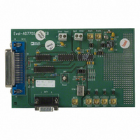
Manufacturer Part Number
EVAL-AD7706EB
Description
BOARD EVAL FOR AD7706
Manufacturer
Analog Devices Inc
Datasheet
1.EVAL-AD7705EB.pdf
(32 pages)
Specifications of EVAL-AD7706EB
Number Of Adc's
1
Number Of Bits
16
Sampling Rate (per Second)
500
Data Interface
Serial
Inputs Per Adc
3 Differential
Input Range
0 ~ 5.25 V
Power (typ) @ Conditions
6.5mW @ 500SPS
Voltage Supply Source
Single
Operating Temperature
-40°C ~ 85°C
Utilized Ic / Part
AD7706
Lead Free Status / RoHS Status
Contains lead / RoHS non-compliant


When operating with a clock frequency of 2.4576 MHz, there is
50 A difference in the current between an externally applied
clock and a crystal resonator when operating with a V
+3 V. With V
current increases by 250 A for a crystal/resonator supplied
clock versus an externally applied clock. The ESR values for
crystals and resonators at this frequency tend to be low and as a
result there tends to be little difference between different crystal
and resonator types.
When operating with a clock frequency of 1 MHz, the ESR
value for different crystal types varies significantly. As a result,
the current drain varies across crystal types. When using a crys-
tal with an ESR of 700
increase in the typical current over an externally-applied clock is
20 A with V
using a crystal with an ESR of 3 k , the increase in the typical
current over an externally applied clock is again 100 A with
V
The on-chip oscillator circuit also has a start-up time associated
with it before it is oscillating at its correct frequency and correct
voltage levels. Typical start-up times with V
using a 4.9512 MHz crystal, 16 ms with a 2.4576 MHz crystal
and 20 ms with a 1 MHz crystal oscillator. Start-up times are
typically 20% slower when the power supply voltage is reduced
to 3 V. At 3 V supplies, depending on the loading capacitances
on the MCLK pins, a 1 M feedback resistor may be required
across the crystal or resonator in order to keep the start up times
around the 20 ms duration.
The AD7705/AD7706’s master clock appears on the MCLK
OUT pin of the device. The maximum recommended load on
this pin is one CMOS load. When using a crystal or ceramic
resonator to generate the AD7705/AD7706’s clock, it may be
desirable to use this clock as the clock source for the system.
In this case, it is recommended that the MCLK OUT signal is
buffered with a CMOS buffer before being applied to the rest of
the circuit.
System Synchronization
The FSYNC bit of the Setup Register allows the user to reset
the modulator and digital filter without affecting any of the
setup conditions on the part. This allows the user to start gath-
ering samples of the analog input from a known point in time,
i.e., when the FSYNC is changed from 1 to 0.
With a 1 in the FSYNC bit of the Setup Register, the digital
filter and analog modulator are held in a known reset state and
the part is not processing any input samples. When a 0 is then
written to the FSYNC bit, the modulator and filter are taken
out of this reset state and the part starts to gather samples again
on the next master clock edge.
The FSYNC input can also be used as a software start convert
command allowing the AD7705/AD7706 to be operated in a
conventional converter fashion. In this mode, writing to the
FSYNC bit starts conversion and the falling edge of DRDY
indicates when conversion is complete. The disadvantage of this
scheme is that the settling time of the filter has to be taken into
account for every data register update. This means that the rate
at which the data register is updated is three times slower in this
mode.
REV. A
DD
= +3 V but 400 A with V
DD
DD
= +3 V and 200 A with V
= +5 V and f
or when using a ceramic resonator, the
CLKIN
DD
= +5 V.
= 2.4576 MHz, the typical
DD
DD
= +5 V. When
= 5 V are 6 ms
DD
of
–21–
Since the FSYNC bit resets the digital filter, the full settling
time of 3
word loaded to the output register on the part. If the DRDY
signal is low when FSYNC goes to a 0, the DRDY signal will
not be reset high by the FSYNC command. This is because the
AD7705/AD7706 recognizes that there is a word in the data
register which has not been read. The DRDY line will stay low
until an update of the data register takes place, at which time it
will go high for 500
from the data register resets the DRDY signal high and it will
not return low until the settling time of the filter has elapsed
(from the FSYNC command) and there is a valid new word in
the data register. If the DRDY line is high when the FSYNC
command is issued, the DRDY line will not return low until the
settling time of the filter has elapsed.
Reset Input
The RESET input on the AD7705/AD7706 resets all the logic,
the digital filter and the analog modulator, while all on-chip
registers are reset to their default state. DRDY is driven high
and the AD7705/AD7706 ignores all communications to any of
its registers while the RESET input is low. When the RESET
input returns high, the AD7705/AD7706 starts to process data
and DRDY will return low in 3
valid new word in the data register. However, the AD7705/
AD7706 operates with its default setup conditions after a
RESET and it is generally necessary to set up all registers and
carry out a calibration after a RESET command.
The AD7705/AD7706’s on-chip oscillator circuit continues to
function even when the RESET input is low. The master clock
signal continues to be available on the MCLK OUT pin. There-
fore, in applications where the system clock is provided by the
AD7705/AD7706’s clock, the AD7705/AD7706 produces an
uninterrupted master clock during RESET commands.
Standby Mode
The STBY bit in the Communications Register of the AD7705/
AD7706 allows the user to place the part in a power-down
mode when it is not required to provide conversion results. The
AD7705/AD7706 retains the contents of all its on-chip registers
(including the data register) while in standby mode. When re-
leased from standby mode, the part starts to process data and a
new word is available in the data register in 3 1/Output rate
from when a 0 is written to the STBY bit.
The STBY bit does not affect the digital interface, nor does it
affect the status of the DRDY line. If DRDY is high when the
STBY bit is brought low, it will remain high until there is a valid
new word in the data register. If DRDY is low when the STBY
bit is brought low, it will remain low until the data register is
updated, at which time the DRDY line will return high for
500 t
the part enters its standby mode (indicating a valid unread word
in the data register), the data register can be read while the part
is in standby. At the end of this read operation, the DRDY will
be reset high as normal.
CLKIN
1/Output Rate has to elapse before there is a new
before returning low again. If DRDY is low when
t
CLKIN
before returning low again. A read
1/Output Rate indicating a
AD7705/AD7706
Related parts for EVAL-AD7706EB
Image
Part Number
Description
Manufacturer
Datasheet
Request
R

Part Number:
Description:
ENERCHIP CC EVAL KIT
Manufacturer:
Cymbet Corporation
Datasheet:

Part Number:
Description:
BOARD EVAL FOR AD976
Manufacturer:
Analog Devices Inc
Datasheet:

Part Number:
Description:
BOARD EVAL FOR ADXL345
Manufacturer:
Analog Devices Inc
Datasheet:

Part Number:
Description:
ENERCHIP CC SEH EVAL KIT
Manufacturer:
Cymbet Corporation
Datasheet:

Part Number:
Description:
ENERCHIP EP ENERGY HARVEST EVAL
Manufacturer:
Cymbet Corporation
Datasheet:

Part Number:
Description:
EVAL BOARD FOR TW6864-LB2-GR
Manufacturer:
Intersil
Datasheet:
Part Number:
Description:
EVAL BOARD FOR TW8816-LB3-GR
Manufacturer:
Intersil
Datasheet:
Part Number:
Description:
EVAL BOARD FOR TW8817-TA3-GRS
Manufacturer:
Intersil
Datasheet:

Part Number:
Description:
EVALUATION MODULE FOR ADUM4160
Manufacturer:
Analog Devices Inc
Datasheet:

Part Number:
Description:
BOARD EVALUATION ADCMP581BCP
Manufacturer:
Analog Devices Inc
Datasheet:
Part Number:
Description:
BOARD EVALUATION ADM1041
Manufacturer:
Analog Devices Inc
Datasheet:

Part Number:
Description:
EVAL BOARD FOR STM32F107VCT
Manufacturer:
STMicroelectronics
Datasheet:
Part Number:
Description:
BOARD EVAL FOR AD1954
Manufacturer:
Analog Devices Inc
Datasheet:
Part Number:
Description:
BOARD EVAL FOR AD1955
Manufacturer:
Analog Devices Inc
Datasheet:

Part Number:
Description:
BOARD EVAL FOR AD7655
Manufacturer:
Analog Devices Inc
Datasheet: