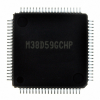
M38D59GCHP#U0 Renesas Electronics America, M38D59GCHP#U0 Datasheet - Page 134

M38D59GCHP#U0
Manufacturer Part Number
M38D59GCHP#U0
Description
IC 740/38D5 MCU QZ-ROM 80LQFP
Manufacturer
Renesas Electronics America
Series
740/38000r
Datasheet
1.M38D58G8FPU0.pdf
(144 pages)
Specifications of M38D59GCHP#U0
Core Processor
740
Core Size
8-Bit
Speed
12.5MHz
Connectivity
SIO, UART/USART
Peripherals
LCD, LED, PWM, WDT
Number Of I /o
59
Program Memory Size
48KB (48K x 8)
Program Memory Type
QzROM
Ram Size
2K x 8
Voltage - Supply (vcc/vdd)
1.8 V ~ 5.5 V
Data Converters
A/D 8x10b
Oscillator Type
Internal
Operating Temperature
-20°C ~ 85°C
Package / Case
80-LQFP
Lead Free Status / RoHS Status
Lead free / RoHS Compliant
Eeprom Size
-
Available stocks
Company
Part Number
Manufacturer
Quantity
Price
38D5 Group
Rev.3.04
REJ03B0158-0304
Notes on Flash Memory Mode
• CPU Rewrite Mode
(1) Operating Speed
During CPU rewrite mode, set the system clock φ to 4.0 MHz or
less using the main clock division ratio selection bits (bits 6 and
7 of address 003B
(2) Prohibited Instructions
During CPU rewrite mode, the instructions which reference data
in the flash memory cannot be used.
(3) Interrupts
During CPU rewrite mode, interrupts cannot be used because
they reference data in the flash memory.
(4) Watchdog Timer
If the watchdog timer has been running already, the internal reset
by underflow will not occur because the watchdog timer is
continuously cleared during program or erase operation.
(5) Reset
Reset is always valid. If CNV
boot mode is active. The program starts from the address stored
in addresses FFFC
Notes on Watchdog Timer
1. Watchdog Timer Underflow
The watchdog timer does not operate in stop mode, but it
continues counting during the wait time to release the stop state
and in wait mode. Write to the watchdog timer control register so
that the watchdog timer will not underflow during these periods.
2. Stopping On-Chip Oscillator Oscillation
When the on-chip oscillator is selected by the watchdog timer
count source selection bit 2, the on-chip oscillator forcibly
oscillates and it cannot be stopped. Also, in this time, set the STP
instruction function selection bit to “1” at this time.
Select “0” ( φ SOURCE) for the watchdog timer count source
selection bit 2 at the system which on-chip oscillator is stopped.
3. Watchdog Timer Control Register
Bits 7 to 5 can be rewritten only once after a reset. After writing,
rewriting is disabled because they are locked. These bits are set
to “0” after a reset.
May 20, 2008 Page 132 of 134
16
16
).
and FFFD
SS
16
= “H” when a reset is released,
in boot ROM area.
Notes on Differences between Flash Memory Version
and QzROM Version
The flash memory and QzROM versions differ in their
manufacturing processes, built-in ROM, memory size, and
layout patterns. Because of these differences, characteristic
values, operation margins, noise immunity, and noise radiation
and oscillation circuit constants may vary within the specified
range of electrical characteristics.
When switching to the QzROM version, implement system
evaluations equivalent to those performed in the flash memory
version.
Confirm page 11 about the differences of functions.
Notes on Power Source Voltage
When the power supply voltage value of the MCU is less than
the value indicated in the recommended operating conditions, the
MCU may not operate normally and perform unstable operation.
In a system where the power source voltage drops slowly when
the power source voltage drops or the power is turned off, reset
the MCU when the power source voltage is less than the
recommended operating conditions, and design the system so
that this unstable operation does not cause errors to it.
Notes on Handling Power Source Pins
Before using the MCU, connect a capacitor suitable for high
frequencies as a bypass capacitor between the following:
The power source pin (V
The power source pin (V
input pin (AV
of 0.01 µ F to 0.1 µ F is recommended.
Also, use the shortest possible wiring to connect a bypass
capacitor between the power source pin and the GND pin and
between the power source pin and the analog power source pin.
Notes on Memory
1. RAM
The RAM content is undefined at a reset. Be sure to set the initial
value before use.
SS
pin). As a bypass capacitor, a ceramic capacitor
CC
CC
pin) and the GND pin (V
pin) and the analog power source
SS
pin)


