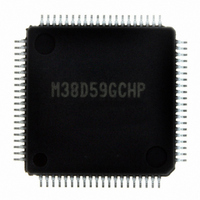
M38D59GCHP#U0 Renesas Electronics America, M38D59GCHP#U0 Datasheet - Page 60

M38D59GCHP#U0
Manufacturer Part Number
M38D59GCHP#U0
Description
IC 740/38D5 MCU QZ-ROM 80LQFP
Manufacturer
Renesas Electronics America
Series
740/38000r
Datasheet
1.M38D58G8FPU0.pdf
(144 pages)
Specifications of M38D59GCHP#U0
Core Processor
740
Core Size
8-Bit
Speed
12.5MHz
Connectivity
SIO, UART/USART
Peripherals
LCD, LED, PWM, WDT
Number Of I /o
59
Program Memory Size
48KB (48K x 8)
Program Memory Type
QzROM
Ram Size
2K x 8
Voltage - Supply (vcc/vdd)
1.8 V ~ 5.5 V
Data Converters
A/D 8x10b
Oscillator Type
Internal
Operating Temperature
-20°C ~ 85°C
Package / Case
80-LQFP
Lead Free Status / RoHS Status
Lead free / RoHS Compliant
Eeprom Size
-
Available stocks
Company
Part Number
Manufacturer
Quantity
Price
38D5 Group
Rev.3.04
REJ03B0158-0304
ROM CORRECTION FUNCTION
A part of program in ROM can be corrected.
Set the start address of the corrected ROM data (i.e. an Op code
address of the beginning instruction) to the ROM correction
address high-order and low-order registers.
When the program is being executed and the value of the
program counter matches with the set address value in the ROM
correction address registers, the program is branched to the ROM
correction vectors and then the correction program can be
executed by setting it to the ROM correction vectors.
Use the JMP instruction (3-byte instruction) to return the main
program from the correction program.
The correctable area is up to two. There are two vectors for ROM
correction.
Also, ROM correction vector can be selected from the RAM area
or ROM area by the ROM correction memory selection bit.
The ROM correction function is controlled by the ROM
correction address 1 enable bit and ROM correction address 2
enable bit.
If the ROM correction function is not used, the ROM correction
vector may be used as normal RAM/ROM. When using the
ROM correction vector as normal RAM/ROM, make sure to set
bits 1 and 0 in the ROM correction enable register to “0”
(Disable).
<Notes>
Fig. 51 Structure of ROM correction enable register
1. When using the ROM correction function, set the ROM cor-
2. Do not set addresses other than the ROM area in the ROM
3. It is necessary to contain the process for ROM correction in
Vector 1
Vector 2
rection address registers and then enable the ROM correc-
tion with the ROM correction enable register.
correction address registers.
Do not set the same ROM correction addresses in both the
ROM correction address registers 1 and ROM correction
address registers 2.
the program.
May 20, 2008 Page 58 of 134
address 0100
address 0120
RAM area
RC2 = “0”
b7
Note: After ROM correction address register is set,
16
16
set the ROM correction address enable bit to be enabled.
address F100
address F120
ROM area
RC2 = “1”
b0
ROM correction enable register (Address 0FFC
RCR
ROM correction address 1 enable bit (RC0)
ROM correction address 2 enable bit (RC1)
ROM correction memory selection bit (RC2)
Not used (returns “0” when read)
16
16
0 : Disable
1 : Enable
0 : Disable
1 : Enable
0 : Branch to the RAM area
1 : Branch to the ROM area
Fig. 49 ROM correction address register
Fig. 50 Memory map of M38D58G8
ROM correction address 1 high-order register (RCA1H)
ROM correction address 1 low-order register (RCA1L)
ROM correction address 2 high-order register (RCA2H)
ROM correction address 2 low-order register (RCA2L)
RAM
ROM
Note: Do not set address other than ROM area.
EFFF
FFDB
FFFF
FF00
063F
F100
F120
0000
0040
0100
8000
8080
0120
16
16
16
16
16
16
16
16
16
16
16
16
16
~ ~
ROM correction vector 1
ROM correction vector 1
ROM correction vector 2
ROM correction vector 2
Reserved ROM area
Reserved ROM area
Interrupt vector area
SFR area
16
)
~ ~
Protect
area 1
Special
page
Zero
page
0FF8
0FF9
0FFA
0FFB
16
16
16
16


