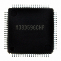
M38D59GCHP#U0 Renesas Electronics America, M38D59GCHP#U0 Datasheet - Page 135

M38D59GCHP#U0
Manufacturer Part Number
M38D59GCHP#U0
Description
IC 740/38D5 MCU QZ-ROM 80LQFP
Manufacturer
Renesas Electronics America
Series
740/38000r
Datasheet
1.M38D58G8FPU0.pdf
(144 pages)
Specifications of M38D59GCHP#U0
Core Processor
740
Core Size
8-Bit
Speed
12.5MHz
Connectivity
SIO, UART/USART
Peripherals
LCD, LED, PWM, WDT
Number Of I /o
59
Program Memory Size
48KB (48K x 8)
Program Memory Type
QzROM
Ram Size
2K x 8
Voltage - Supply (vcc/vdd)
1.8 V ~ 5.5 V
Data Converters
A/D 8x10b
Oscillator Type
Internal
Operating Temperature
-20°C ~ 85°C
Package / Case
80-LQFP
Lead Free Status / RoHS Status
Lead free / RoHS Compliant
Eeprom Size
-
Available stocks
Company
Part Number
Manufacturer
Quantity
Price
38D5 Group
Rev.3.04
REJ03B0158-0304
Notes on QzROM Version
Wiring to OSCSEL pin
(1) OSCSEL = L
Connect the OSCSEL pin the shortest possible to the GND
pattern which is supplied to the V
addition connecting an approximately 5 k Ω resistor in series to
the GND could improve noise immunity. In this case as well as
the above mention, connect the pin the shortest possible to the
GND pattern which is supplied to the V
microcomputer.
(2) OSCSEL = H
Connect the OSCSEL pin the shortest possible to the V
which is supplied to the V
addition connecting an approximately 5 k Ω resistor in series to
the V
the above mention, connect the pin the shortest possible to the
V
microcomputer.
<Reason>
The OSCSEL pin is the power source input pin for the built-in
QzROM.
When programming in the QzROM, the impedance of the
OSCSEL pin is low to allow the electric current for writing to
flow into the built-in QzROM. Because of this, noise can enter
easily. If noise enters the OSCSEL pin, abnormal instruction
codes or data are read from the QzROM, which may cause a
program runaway.
Fig. 107 Wiring for OSCSEL pin
Overvoltage in QzROM Version
Make sure that voltage exceeding the V
applied to other pins. In particular, ensure that the state indicated
by bold lines in figure below does not occur for pin OSCSEL pin
(V
off. Otherwise the contents of QzROM could be rewritten.
Fig. 108 Timing Diagram (Bold-lined periods are applicable)
V
OSCSEL pin voltage
“H” input
OSCSEL pin voltage
“L” input
C C
PP
CC
Termination of OSCSEL pin
pin voltage
power source pin for QzROM) during power-on or power-
CC
p a t t e r n w h i c h i s s u p p l i e d t o t h e V
(1) OSCSEL = L
could improve noise immunity. In this case as well as
Note 1 : It shows the microcomputer’s pin
OSCSEL
May 20, 2008 Page 133 of 134
(1) Input voltage to other MCU pins rises before V
(2) Input voltage to other MCU pins falls after V
Note: The internal circuitry is unstable when V
V
1.8V
SS
voltage specification of 1.8 V (shaded portion), so particular care should
be exercised regarding overvoltage.
(1)
(1)
The shortest
The shortest
(1)
about 5 k Ω
CC
pin of the microcomputer. In
SS
(2) OSCSEL = H
pin of the microcomputer. In
OSCSEL
CC
CC
CC
V
is below the minimum
CC
pin voltage.
CC
pin voltage is not
pin voltage.
(1)
(1)
C C
S S
(2)
The shortest
The shortest
pin of the
p i n o f t h e
about 5 k Ω
CC
1.8V
pattern
QzROM Version Product Shipped in Blank
As for the product shipped in blank, Renesas does not perform
the writing test to user ROM area after the assembly process
though the QzROM writing test is performed enough before the
assembly process. Therefore, a writing error of approximate
0.1% may occur.
Moreover, please note the contact of cables and foreign bodies on
a socket, etc. because a writing environment may cause some
writing errors.
Ordering QzROM Writing
1. Notes On QzROM Writing Orders
When ordering the QzROM product shipped after writing,
submit the mask file (extension: .msk) which is made by the
mask file converter MM.
• Be sure to set the ROM option data* setup when making the
• Set “FF
* ROM option data: mask option noted in MM
2. Data Required for QzROM Ordering
The following are necessary when ordering a QzROM product
shipped after writing:
* For the QzROM writing confirmation form and the mark
specification form, refer to the “Renesas Technology Corp.”
Homepage (http://www.renesas.com/homepage.jsp).
Note that we cannot deal with special font marking (customer's
trademark etc.) in QzROM microcomputer.
3. QzROM Product Receiving Procedure
When writing to QzROM is performed by user side, the
receiving inspection by the following flow is necessary.
Fig. 109 QzROM receiving procedure
mask file by using the mask file converter MM.. The ROM
code protect is specified according to the ROM option data* in
the mask file which is submitted at ordering. Note that the
mask file which has nothing at the ROM option data* or has
the data other than “00
accepted.
regardless of the presence or absence of a protect. When data
other than “FF
submitted again.
QzROM product shipped after writing
“protect disabled”
“protect enabled to the protect area 1”
• QzROM Writing Confirmation Form*
• Mark Specification Form*
• ROM data: Mask file
Programming to unprotected area
Verify test for unprotected area
Renesas
unprotected area (Verify test)
User
Receiving inspection of
16
” to the ROM code protect address in ROM data
Programming
Verify test
16
” is set, we may ask that the ROM data be
Shipping
16
”, “FE
QzROM product shipped in blank
16
” and “FF
Renesas
User
Verify test for all area
Receiving inspection
(Blank check)
Programming
16
Shipping
” can not be


