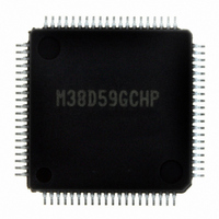
M38D59GCHP#U0 Renesas Electronics America, M38D59GCHP#U0 Datasheet - Page 137

M38D59GCHP#U0
Manufacturer Part Number
M38D59GCHP#U0
Description
IC 740/38D5 MCU QZ-ROM 80LQFP
Manufacturer
Renesas Electronics America
Series
740/38000r
Datasheet
1.M38D58G8FPU0.pdf
(144 pages)
Specifications of M38D59GCHP#U0
Core Processor
740
Core Size
8-Bit
Speed
12.5MHz
Connectivity
SIO, UART/USART
Peripherals
LCD, LED, PWM, WDT
Number Of I /o
59
Program Memory Size
48KB (48K x 8)
Program Memory Type
QzROM
Ram Size
2K x 8
Voltage - Supply (vcc/vdd)
1.8 V ~ 5.5 V
Data Converters
A/D 8x10b
Oscillator Type
Internal
Operating Temperature
-20°C ~ 85°C
Package / Case
80-LQFP
Lead Free Status / RoHS Status
Lead free / RoHS Compliant
Eeprom Size
-
Available stocks
Company
Part Number
Manufacturer
Quantity
Price
Rev.
1.00
2.00
REVISION HISTORY
REVISION HISTORY
Aug 12, 2005
Jan 23, 2006
Date
61-65
Page
13
14
15
22
52
53
55
57
58
59
60
68
69
−
−
−
−
−
1
6
7
First edition issued
Pin name revised: CNVss → OSCSEL
Frequency name revised: ROSC → OCO
Mode name revised: Middle-, High-speed mode → Frequency/2, 4, 8 mode
Bit names of some registers:
1. ROSC stop bit → On-chip oscillator stop bit
2. STP instruction disable bit → STP instruction function selection bit
3. Vector 1 enable bit (RC0) → ROM correction address 1 enable bit (RC0)
4. Vector 2 enable bit (RC1) → ROM correction address 2 enable bit (RC1)
5. Vector control bit (RC2) → ROM correction memory selection bit (RC2)
Description, Power source voltage and Power dissipation revised.
Table 2 Pin description (1): Some description of Port P1 Function revised.
Table 3 Pin description (2): Description of OSCSEL added.
Fig. 5 Memory expansion plan, Table 4 Support products
M38D59GFFP/HP, M38D59GCFP/HP added.
Some description revised.
Fig. 8 Structure of CPU mode register: Note on on-chip oscillator added.
Fig. 9 Switch procedure of CPU mode register: Initial values of CPUM2 added and
initial value of CPUM revised.
Fig. 10 Memory map diagram:
Reserved ROM area FFD4
Note on ROM correction vector added.
Fig. 11 Memory map of special function register (SFR):
“Reserved area” is added to address 0FFD
Table 8 Termination of unused pins: X
ROM CORRECTION FUNCTION:
Description and some bit names revised and Fig. 47 Memory map of M38D58 added.
Initial Value of Watchdog Timer: Some description added.
Standard Operation of Watchdog Timer: Some description eliminated.
Bit 6 of Watchdog Timer Control Register added.
Note 2 revised.
Fig. 50 Structure of Watchdog timer control register:
Name of bit 6 and description of its function revised.
Fig. 55 Reset sequence revised.
Fig. 56 Internal state at reset: ROM correction address 1 (low-order), ROM
correction address 2 (high-order) and ROM correction address 2 (low-order)
revised.
Oscillation Control (1) Stop Mode: Some description revised.
Fig. 58 Clock generating circuit block diagram:
“or ROSC clock division ratio selection bit” eliminated.
Fig. 60 State transitions of system clock
on-chip oscillator mode: f(OCO) → f(OCO)/32,
Note 8 to Note 10 revised and Note 12 added.
QzROM programming mode (Overview, Pin description, Pin connection diagram,
Connection example) added.
(6) Wiring to OSCSEL pin revised.
QzROM Receive Flow added.
(1/7)
16
38D5 Group Data Sheet
to FFDC
Description
Summary
IN
16
and X
→ FFD0
16
, and Note added.
OUT
16
pin termination added.
to FFDC
16


