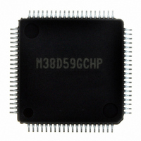
M38D59GCHP#U0 Renesas Electronics America, M38D59GCHP#U0 Datasheet - Page 95

M38D59GCHP#U0
Manufacturer Part Number
M38D59GCHP#U0
Description
IC 740/38D5 MCU QZ-ROM 80LQFP
Manufacturer
Renesas Electronics America
Series
740/38000r
Datasheet
1.M38D58G8FPU0.pdf
(144 pages)
Specifications of M38D59GCHP#U0
Core Processor
740
Core Size
8-Bit
Speed
12.5MHz
Connectivity
SIO, UART/USART
Peripherals
LCD, LED, PWM, WDT
Number Of I /o
59
Program Memory Size
48KB (48K x 8)
Program Memory Type
QzROM
Ram Size
2K x 8
Voltage - Supply (vcc/vdd)
1.8 V ~ 5.5 V
Data Converters
A/D 8x10b
Oscillator Type
Internal
Operating Temperature
-20°C ~ 85°C
Package / Case
80-LQFP
Lead Free Status / RoHS Status
Lead free / RoHS Compliant
Eeprom Size
-
Available stocks
Company
Part Number
Manufacturer
Quantity
Price
38D5 Group
Rev.3.04
REJ03B0158-0304
NOTES ON USE
Processor Status Register
The contents of the processor status register (PS) after a reset are
undefined, except for the interrupt disable flag (I) which is “1”.
After a reset, initialize flags which affect program execution.
In particular, it is essential to initialize the index X mode (T) and
the decimal mode (D) flags because of their effect on
calculations. Initialize these flags at beginning of the program.
Interrupt
The contents of the interrupt request bits do not change
immediately after they have been written. After writing to an
interrupt request register, execute at least one instruction before
performing a BBC or BBS instruction.
Decimal Calculations
• To calculate in decimal notation, set the decimal mode flag (D)
• In decimal mode, the values of the negative (N), overflow (V),
Timers
The division ratio is 1/(n+1) when the value n (0 to 255) is
written to the timer latch.
Multiplication and Division Instructions
The index mode (T) and the decimal mode (D) flags do not affect
the MUL and DIV instruction.
The execution of these instructions does not change the contents
of the processor status register.
Direction Registers
The values of the port direction registers cannot be read. This
means, it is impossible to use the LDA instruction, memory
operation instruction when the T flag is “1”, addressing mode
using direction register values as qualifiers, and bit test
instructions such as BBC and BBS. It is also impossible to use bit
operation instructions such as CLB and SEB, and read-modify-
write instructions to direction registers, including calculations
such as ROR. To set the direction registers, use instructions such
as LDM or STA.
Serial Interface
In clock synchronous serial I/O, if the receive side is using an
external clock and it is to output the S
enable bit, the receive enable bit, and the S
to “1”.
Serial I/O continues to output the final bit from the T
transmission is completed.
to “1”, then execute an ADC or SBC instruction. After
executing an ADC or SBC instruction, execute at least one
instruction before executing a SEC, CLC, or CLD instruction.
and zero (Z) flags are invalid.
May 20, 2008 Page 93 of 134
RDY
signal, set the transmit
RDY
output enable bit
X
D pin after
A/D Converter
The comparator is constructed linked to a capacitor. The
conversion accuracy may be low because the charge is lost if the
conversion speed is not enough. Accordingly, set f(X
least 500kHz during A/D conversion in the X
Also, do not execute the STP or WIT instruction during an A/D
conversion.
In the low-speed mode, since the A/D conversion is executed by
the on-chip oscillator, the minimum value of f(X
not limited.
LCD Drive Control Circuit
Execution of the STP instruction sets the LCD enable bit (bit 4 of
the LCD mode register) to “0” and the LCD panel turns off. To
make the LCD panel turn on after returning from the stop mode,
set the LCD enable bit to “1”.
Instruction Execution Time
The instruction execution time is obtained by multiplying the
frequency of the internal clock φ by the number of cycles needed
to execute an instruction.
The number of cycles required to execute an instruction is shown
in the list of machine instructions.
Power Source Voltage
When the power source voltage value of a microcomputer is less
than the value which is indicated as the recommended operating
conditions, the microcomputer does not operate normally and
may perform unstable operation.
In a system where the power source voltage drops slowly when
the power source voltage drops or the power supply is turned off,
reset a microcomputer when the power source voltage is less
than the recommended operating conditions and design a system
not to cause errors to the system by this unstable operation.
Handling of Power Source Pin
In order to avoid a latch-up occurrence, connect a capacitor
suitable for high frequencies as bypass capacitor between power
source pin (V
source pin (V
Besides, connect the capacitor to as close as possible. For bypass
capacitor which should not be located too far from the pins to be
connected, a ceramic capacitor of 0.1 µ F is recommended.
LCD drive power supply
Power supply capacitor may be insufficient with the division
resistance for LCD power supply, and the characteristic of the
LCD panel. In this case, there is the method of connecting the
bypass capacitor about 0.1 − 0.33 µ F to V
example of a strengthening measure of the LCD drive power
supply is shown below.
Fig. 86 Strengthening measure example of LCD drive
power supply
CC
CC
pin) and GND pin (Vss pin), and between power
pin) and analog power source pin (AV
V
V
V
L2
L1
L3
• Connect by the shortest
• Connect the bypass capacitor
(Referential value:0.1−0.33 µF)
possible wiring.
to the V
as possible.
L1
−V
L1
IN
L3
mode.
− V
IN
pins as short
) frequency is
L3
pins. The
IN
) to at
CC
).


