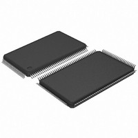
AT91SAM7SE256-AU Atmel, AT91SAM7SE256-AU Datasheet - Page 146

AT91SAM7SE256-AU
Manufacturer Part Number
AT91SAM7SE256-AU
Description
IC ARM7 MCU FLASH 256K 128-LQFP
Manufacturer
Atmel
Series
AT91SAMr
Datasheets
1.AT88SC-SDK1.pdf
(90 pages)
2.AT91SAM7SE256-AU.pdf
(673 pages)
3.AT91SAM7SE32-AU.pdf
(655 pages)
Specifications of AT91SAM7SE256-AU
Core Processor
ARM7
Core Size
16/32-Bit
Speed
55MHz
Connectivity
EBI/EMI, I²C, SPI, SSC, UART/USART, USB
Peripherals
Brown-out Detect/Reset, POR, PWM, WDT
Number Of I /o
88
Program Memory Size
256KB (256K x 8)
Program Memory Type
FLASH
Ram Size
32K x 8
Voltage - Supply (vcc/vdd)
1.65 V ~ 1.95 V
Data Converters
A/D 8x10b
Oscillator Type
Internal
Operating Temperature
-40°C ~ 85°C
Package / Case
128-LQFP
Processor Series
AT91SAMx
Core
ARM7TDMI
Data Bus Width
32 bit
Data Ram Size
32 KB
Interface Type
SPI, TWI, USART
Maximum Clock Frequency
55 MHz
Number Of Programmable I/os
88
Number Of Timers
2
Operating Supply Voltage
3 V to 3.6 V
Maximum Operating Temperature
+ 85 C
Mounting Style
SMD/SMT
3rd Party Development Tools
JTRACE-ARM-2M, KSK-AT91SAM7S-PL, MDK-ARM, RL-ARM, ULINK2
Development Tools By Supplier
AT91SAM-ICE, AT91-ISP, AT91SAM7SE-EK
Minimum Operating Temperature
- 40 C
On-chip Adc
10 bit, 8 Channel
Controller Family/series
AT91SAM7xxxxx
No. Of I/o's
88
Ram Memory Size
32KB
Cpu Speed
48MHz
No. Of Timers
3
Rohs Compliant
Yes
For Use With
AT91SAM7SE-EK - EVAL BOARD FOR AT91SAM7SEAT91SAM-ICE - EMULATOR FOR AT91 ARM7/ARM9
Lead Free Status / RoHS Status
Lead free / RoHS Compliant
Eeprom Size
-
Lead Free Status / Rohs Status
Lead free / RoHS Compliant
Available stocks
Company
Part Number
Manufacturer
Quantity
Price
Company:
Part Number:
AT91SAM7SE256-AU
Manufacturer:
ATMEL
Quantity:
165
- Current page: 146 of 673
- Download datasheet (11Mb)
21.6.6
Figure 21-6. NAND Flash Signal Multiplexing on EBI Pins
146
SMC
SAM7SE512/256/32 Preliminary
NAND Flash Support
NWR0_NWE
NCS3
NRD
The EBI integrates circuitry that interfaces to NAND Flash devices.
The NAND Flash logic is driven by the Static Memory Controller on the NCS3 address space.
Programming the CS3A field in the Chip Select Assignment Register to the appropriate value
enables the NAND Flash logic
Access to an external NAND Flash device is then made by accessing the address space
reserved to NCS3 (i.e., between 0x4000 0000 and 0x4FFF FFFF).
The NAND Flash Logic drives the read and write command signals of the SMC on the NANDOE
and NANDWE signals when the NCS3 signal is active. NANDOE and NANDWE are invalidated
as soon as the transfer address fails to lie in the NCS3 address space. For details on these
waveforms, refer to the Static Memory Controller Section.
(1)
enabled (default state after reset) or as PIO Output set at logic level 1. The PIO cannot be used in PIO
Mode.
The address latch enable and command latch enable signals on the NAND Flash device are
driven respectively by address bits A21 and A22 of the EBI address bus. The command,
address or data words on the data bus of the NAND Flash device are distinguished by using
their address within the NCS3 address space. The chip enable (CE) signal of the device and the
ready/busy (R/B) signals are connected to PIO lines. The CE signal then remains asserted even
when NCS3 is not selected, preventing the device from returning to standby mode.
(1)
When the NAND Flash Logic is used, NWR0/NWE/CFWE must be kept as PIO Input Mode with Pull-up
NAND Flash Logic
(See “EBI Chip Select Assignment Register” on page
NANDOE
NANDWE
MUX Logic
CS3A
CS3A
6222F–ATARM–14-Jan-11
NANDOE
NANDWE
158.).
Related parts for AT91SAM7SE256-AU
Image
Part Number
Description
Manufacturer
Datasheet
Request
R

Part Number:
Description:
EVAL BOARD FOR AT91SAM7SE
Manufacturer:
Atmel
Datasheet:

Part Number:
Description:
KIT EVAL FOR ARM AT91SAM7S
Manufacturer:
Atmel
Datasheet:

Part Number:
Description:
MCU, MPU & DSP Development Tools KICKSTART KIT ATMEL AT91SAM7S
Manufacturer:
IAR Systems

Part Number:
Description:
MCU ARM9 64K SRAM 144-LFBGA
Manufacturer:
Atmel
Datasheet:

Part Number:
Description:
IC ARM7 MCU FLASH 256K 100LQFP
Manufacturer:
Atmel
Datasheet:

Part Number:
Description:
IC ARM9 MPU 217-LFBGA
Manufacturer:
Atmel
Datasheet:

Part Number:
Description:
MCU ARM9 ULTRA LOW PWR 217-LFBGA
Manufacturer:
Atmel
Datasheet:

Part Number:
Description:
MCU ARM9 324-TFBGA
Manufacturer:
Atmel
Datasheet:

Part Number:
Description:
IC MCU ARM9 SAMPLING 217CBGA
Manufacturer:
Atmel
Datasheet:

Part Number:
Description:
IC ARM9 MCU 217-LFBGA
Manufacturer:
Atmel
Datasheet:

Part Number:
Description:
IC ARM9 MCU 208-PQFP
Manufacturer:
Atmel
Datasheet:

Part Number:
Description:
MCU ARM 512K HS FLASH 100-LQFP
Manufacturer:
Atmel
Datasheet:

Part Number:
Description:
MCU ARM 512K HS FLASH 100-TFBGA
Manufacturer:
Atmel
Datasheet:

Part Number:
Description:
IC ARM9 MCU 200 MHZ 324-TFBGA
Manufacturer:
Atmel
Datasheet:

Part Number:
Description:
IC ARM MCU 16BIT 128K 256BGA
Manufacturer:
Atmel
Datasheet:


