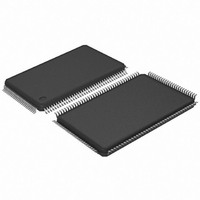
AT91SAM7SE256-AU Atmel, AT91SAM7SE256-AU Datasheet - Page 174

AT91SAM7SE256-AU
Manufacturer Part Number
AT91SAM7SE256-AU
Description
IC ARM7 MCU FLASH 256K 128-LQFP
Manufacturer
Atmel
Series
AT91SAMr
Datasheets
1.AT88SC-SDK1.pdf
(90 pages)
2.AT91SAM7SE256-AU.pdf
(673 pages)
3.AT91SAM7SE32-AU.pdf
(655 pages)
Specifications of AT91SAM7SE256-AU
Core Processor
ARM7
Core Size
16/32-Bit
Speed
55MHz
Connectivity
EBI/EMI, I²C, SPI, SSC, UART/USART, USB
Peripherals
Brown-out Detect/Reset, POR, PWM, WDT
Number Of I /o
88
Program Memory Size
256KB (256K x 8)
Program Memory Type
FLASH
Ram Size
32K x 8
Voltage - Supply (vcc/vdd)
1.65 V ~ 1.95 V
Data Converters
A/D 8x10b
Oscillator Type
Internal
Operating Temperature
-40°C ~ 85°C
Package / Case
128-LQFP
Processor Series
AT91SAMx
Core
ARM7TDMI
Data Bus Width
32 bit
Data Ram Size
32 KB
Interface Type
SPI, TWI, USART
Maximum Clock Frequency
55 MHz
Number Of Programmable I/os
88
Number Of Timers
2
Operating Supply Voltage
3 V to 3.6 V
Maximum Operating Temperature
+ 85 C
Mounting Style
SMD/SMT
3rd Party Development Tools
JTRACE-ARM-2M, KSK-AT91SAM7S-PL, MDK-ARM, RL-ARM, ULINK2
Development Tools By Supplier
AT91SAM-ICE, AT91-ISP, AT91SAM7SE-EK
Minimum Operating Temperature
- 40 C
On-chip Adc
10 bit, 8 Channel
Controller Family/series
AT91SAM7xxxxx
No. Of I/o's
88
Ram Memory Size
32KB
Cpu Speed
48MHz
No. Of Timers
3
Rohs Compliant
Yes
For Use With
AT91SAM7SE-EK - EVAL BOARD FOR AT91SAM7SEAT91SAM-ICE - EMULATOR FOR AT91 ARM7/ARM9
Lead Free Status / RoHS Status
Lead free / RoHS Compliant
Eeprom Size
-
Lead Free Status / Rohs Status
Lead free / RoHS Compliant
Available stocks
Company
Part Number
Manufacturer
Quantity
Price
Company:
Part Number:
AT91SAM7SE256-AU
Manufacturer:
ATMEL
Quantity:
165
- Current page: 174 of 673
- Download datasheet (11Mb)
22.6.5
22.6.5.1
Figure 22-19. Read Access with Setup and Hold
174
A[22:0]
MCK
NRD
SAM7SE512/256/32 Preliminary
Setup and Hold Cycles
Read Access
The SMC allows some memory devices to be interfaced with different setup, hold and pulse
delays. These parameters are programmable and define the timing of each portion of the read
and write cycles. However, it is not possible to use this feature in early read protocol.
If an attempt is made to program the setup parameter as not equal to zero and the hold parame-
ter as equal to zero with WSEN = 0 (0 standard wait state), the SMC does not operate correctly.
If consecutive accesses are made to two different external memories and the second memory is
programmed with setup cycles, then no chip select change wait state is inserted (see
23 on page
When a data float wait state (t
memory bank is programmed with setup cycles, the SMC behaves as follows:
The read cycle can be divided into a setup, a pulse length and a hold. The setup parameter can
have a value between 1.5 and 7.5 clock cycles, the hold parameter between 0 and 7 clock
cycles and the pulse length between 1.5 and 128.5 clock cycles, by increments of one.
Figure 22-20. Read Access with Setup
• If the number of t
• If the number of the setup cycle is higher than the number of t
NRD Setup
cycles inserted is equal to 0 (see
0 (see
A[22:0]
Figure 22-25 on page
MCK
NRD
176).
DF
is higher or equal to the number of setup cycles, the number of setup
DF
) is programmed on the first memory bank and when the second
177).
NRD Setup
Figure 22-24 on page
Pulse Length
176).
Pulse Length
DF,
the number of t
NRD Hold
6222F–ATARM–14-Jan-11
DF
inserted is
Figure 22-
Related parts for AT91SAM7SE256-AU
Image
Part Number
Description
Manufacturer
Datasheet
Request
R

Part Number:
Description:
EVAL BOARD FOR AT91SAM7SE
Manufacturer:
Atmel
Datasheet:

Part Number:
Description:
KIT EVAL FOR ARM AT91SAM7S
Manufacturer:
Atmel
Datasheet:

Part Number:
Description:
MCU, MPU & DSP Development Tools KICKSTART KIT ATMEL AT91SAM7S
Manufacturer:
IAR Systems

Part Number:
Description:
MCU ARM9 64K SRAM 144-LFBGA
Manufacturer:
Atmel
Datasheet:

Part Number:
Description:
IC ARM7 MCU FLASH 256K 100LQFP
Manufacturer:
Atmel
Datasheet:

Part Number:
Description:
IC ARM9 MPU 217-LFBGA
Manufacturer:
Atmel
Datasheet:

Part Number:
Description:
MCU ARM9 ULTRA LOW PWR 217-LFBGA
Manufacturer:
Atmel
Datasheet:

Part Number:
Description:
MCU ARM9 324-TFBGA
Manufacturer:
Atmel
Datasheet:

Part Number:
Description:
IC MCU ARM9 SAMPLING 217CBGA
Manufacturer:
Atmel
Datasheet:

Part Number:
Description:
IC ARM9 MCU 217-LFBGA
Manufacturer:
Atmel
Datasheet:

Part Number:
Description:
IC ARM9 MCU 208-PQFP
Manufacturer:
Atmel
Datasheet:

Part Number:
Description:
MCU ARM 512K HS FLASH 100-LQFP
Manufacturer:
Atmel
Datasheet:

Part Number:
Description:
MCU ARM 512K HS FLASH 100-TFBGA
Manufacturer:
Atmel
Datasheet:

Part Number:
Description:
IC ARM9 MCU 200 MHZ 324-TFBGA
Manufacturer:
Atmel
Datasheet:

Part Number:
Description:
IC ARM MCU 16BIT 128K 256BGA
Manufacturer:
Atmel
Datasheet:


