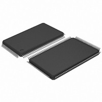
AT91SAM7SE256-AU Atmel, AT91SAM7SE256-AU Datasheet - Page 556

AT91SAM7SE256-AU
Manufacturer Part Number
AT91SAM7SE256-AU
Description
IC ARM7 MCU FLASH 256K 128-LQFP
Manufacturer
Atmel
Series
AT91SAMr
Datasheets
1.AT88SC-SDK1.pdf
(90 pages)
2.AT91SAM7SE256-AU.pdf
(673 pages)
3.AT91SAM7SE32-AU.pdf
(655 pages)
Specifications of AT91SAM7SE256-AU
Core Processor
ARM7
Core Size
16/32-Bit
Speed
55MHz
Connectivity
EBI/EMI, I²C, SPI, SSC, UART/USART, USB
Peripherals
Brown-out Detect/Reset, POR, PWM, WDT
Number Of I /o
88
Program Memory Size
256KB (256K x 8)
Program Memory Type
FLASH
Ram Size
32K x 8
Voltage - Supply (vcc/vdd)
1.65 V ~ 1.95 V
Data Converters
A/D 8x10b
Oscillator Type
Internal
Operating Temperature
-40°C ~ 85°C
Package / Case
128-LQFP
Processor Series
AT91SAMx
Core
ARM7TDMI
Data Bus Width
32 bit
Data Ram Size
32 KB
Interface Type
SPI, TWI, USART
Maximum Clock Frequency
55 MHz
Number Of Programmable I/os
88
Number Of Timers
2
Operating Supply Voltage
3 V to 3.6 V
Maximum Operating Temperature
+ 85 C
Mounting Style
SMD/SMT
3rd Party Development Tools
JTRACE-ARM-2M, KSK-AT91SAM7S-PL, MDK-ARM, RL-ARM, ULINK2
Development Tools By Supplier
AT91SAM-ICE, AT91-ISP, AT91SAM7SE-EK
Minimum Operating Temperature
- 40 C
On-chip Adc
10 bit, 8 Channel
Controller Family/series
AT91SAM7xxxxx
No. Of I/o's
88
Ram Memory Size
32KB
Cpu Speed
48MHz
No. Of Timers
3
Rohs Compliant
Yes
For Use With
AT91SAM7SE-EK - EVAL BOARD FOR AT91SAM7SEAT91SAM-ICE - EMULATOR FOR AT91 ARM7/ARM9
Lead Free Status / RoHS Status
Lead free / RoHS Compliant
Eeprom Size
-
Lead Free Status / Rohs Status
Lead free / RoHS Compliant
Available stocks
Company
Part Number
Manufacturer
Quantity
Price
Company:
Part Number:
AT91SAM7SE256-AU
Manufacturer:
ATMEL
Quantity:
165
- Current page: 556 of 673
- Download datasheet (11Mb)
38.2
Figure 38-1. Block Diagram
38.2.1
556
MCK
UDPCK
udp_int
Block Diagram
SAM7SE512/256/32 Preliminary
Atmel Bridge
MCU
APB
Signal Description
Bus
to
Access to the UDP is via the APB bus interface. Read and write to the data FIFO are done by
reading and writing 8-bit values to APB registers.
The UDP peripheral requires two clocks: one peripheral clock used by the Master Clock domain
(MCK) and a 48 MHz clock (UDPCK) used by the 12 MHz domain.
A USB 2.0 full-speed pad is embedded and controlled by the Serial Interface Engine (SIE).
The signal external_resume is optional. It allows the UDP peripheral to wake up once in system
mode. The host is then notified that the device asks for a resume. This optional feature must
also be negotiated with the host during the enumeration.
Table 38-2.
Signal Name
UDPCK
MCK
udp_int
DDP
DDM
U
e
n
e
a
e
s
c
r
I
t
r
f
Signal Names
W
a
p
p
e
Master Clock
Domain
r
r
USB Device
RAM
FIFO
Dual
Port
Description
48 MHz clock
Master clock
Interrupt line connected to the Advanced Interrupt
Controller (AIC)
USB D+ line
USB D- line
Recovered 12 MHz
Domain
W
a
p
p
e
r
r
Suspend/Resume Logic
12 MHz
Interface
Engine
Serial
SIE
txoen
eopn
txd
rxdm
rxd
rxdp
6222F–ATARM–14-Jan-11
Type
input
input
input
I/O
I/O
Transceiver
Embedded
USB
DDM
DDP
Related parts for AT91SAM7SE256-AU
Image
Part Number
Description
Manufacturer
Datasheet
Request
R

Part Number:
Description:
EVAL BOARD FOR AT91SAM7SE
Manufacturer:
Atmel
Datasheet:

Part Number:
Description:
KIT EVAL FOR ARM AT91SAM7S
Manufacturer:
Atmel
Datasheet:

Part Number:
Description:
MCU, MPU & DSP Development Tools KICKSTART KIT ATMEL AT91SAM7S
Manufacturer:
IAR Systems

Part Number:
Description:
MCU ARM9 64K SRAM 144-LFBGA
Manufacturer:
Atmel
Datasheet:

Part Number:
Description:
IC ARM7 MCU FLASH 256K 100LQFP
Manufacturer:
Atmel
Datasheet:

Part Number:
Description:
IC ARM9 MPU 217-LFBGA
Manufacturer:
Atmel
Datasheet:

Part Number:
Description:
MCU ARM9 ULTRA LOW PWR 217-LFBGA
Manufacturer:
Atmel
Datasheet:

Part Number:
Description:
MCU ARM9 324-TFBGA
Manufacturer:
Atmel
Datasheet:

Part Number:
Description:
IC MCU ARM9 SAMPLING 217CBGA
Manufacturer:
Atmel
Datasheet:

Part Number:
Description:
IC ARM9 MCU 217-LFBGA
Manufacturer:
Atmel
Datasheet:

Part Number:
Description:
IC ARM9 MCU 208-PQFP
Manufacturer:
Atmel
Datasheet:

Part Number:
Description:
MCU ARM 512K HS FLASH 100-LQFP
Manufacturer:
Atmel
Datasheet:

Part Number:
Description:
MCU ARM 512K HS FLASH 100-TFBGA
Manufacturer:
Atmel
Datasheet:

Part Number:
Description:
IC ARM9 MCU 200 MHZ 324-TFBGA
Manufacturer:
Atmel
Datasheet:

Part Number:
Description:
IC ARM MCU 16BIT 128K 256BGA
Manufacturer:
Atmel
Datasheet:


