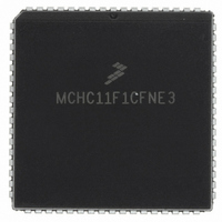
MCHC11F1CFNE3 Freescale Semiconductor, MCHC11F1CFNE3 Datasheet - Page 21

MCHC11F1CFNE3
Manufacturer Part Number
MCHC11F1CFNE3
Description
IC MCU 8BIT 1K RAM 68-PLCC
Manufacturer
Freescale Semiconductor
Series
HC11r
Specifications of MCHC11F1CFNE3
Core Processor
HC11
Core Size
8-Bit
Speed
3MHz
Connectivity
SCI, SPI
Peripherals
POR, WDT
Number Of I /o
30
Program Memory Type
ROMless
Eeprom Size
512 x 8
Ram Size
1K x 8
Voltage - Supply (vcc/vdd)
4.75 V ~ 5.25 V
Data Converters
A/D 8x8b
Oscillator Type
Internal
Operating Temperature
-40°C ~ 85°C
Package / Case
68-PLCC
A/d Inputs
8-Channel, 8-Bit
Eeprom Memory
512 Bytes
Input Output
30
Interface
SCI/SPI
Memory Type
EPROM
Number Of Bits
8
Package Type
68-pin PLCC
Programmable Memory
0 Bytes
Timers
3-16-bit
Voltage, Range
3-5.5 V
Controller Family/series
68HC11
No. Of I/o's
30
Eeprom Memory Size
512Byte
Ram Memory Size
1KB
Cpu Speed
3MHz
No. Of Timers
1
Embedded Interface Type
SCI, SPI
Rohs Compliant
Yes
Processor Series
HC11F
Core
HC11
Data Bus Width
8 bit
Program Memory Size
512 B
Data Ram Size
1 KB
Interface Type
SCI, SPI
Maximum Clock Frequency
3 MHz
Number Of Timers
1
Maximum Operating Temperature
+ 85 C
Mounting Style
SMD/SMT
Minimum Operating Temperature
- 40 C
On-chip Adc
8 bit, 8 Channel
Lead Free Status / RoHS Status
Lead free / RoHS Compliant
Program Memory Size
-
Lead Free Status / Rohs Status
RoHS Compliant part
Available stocks
Company
Part Number
Manufacturer
Quantity
Price
Company:
Part Number:
MCHC11F1CFNE3
Manufacturer:
FREESCALE
Quantity:
5 530
Company:
Part Number:
MCHC11F1CFNE3
Manufacturer:
FREESCALE
Quantity:
5 530
Company:
Part Number:
MCHC11F1CFNE3
Manufacturer:
Freescale Semiconductor
Quantity:
10 000
Company:
Part Number:
MCHC11F1CFNE3R
Manufacturer:
Freescale Semiconductor
Quantity:
10 000
2.11.1 Port A
TECHNICAL DATA
Port A is an 8-bit general-purpose I/O port with a data register (PORTA) and a data
direction register (DDRA). Port A pins share functions with the 16-bit timer system.
PORTA can be read at any time. Inputs return the pin level; outputs return the pin driv-
er input level. If written, PORTA stores the data in internal latches. It drives the pins
only if they are configured as outputs. Writes to PORTA do not change the pin state
when the pins are configured for timer output compares.
Out of reset, port A pins [7:0] are general-purpose high-impedance inputs. When the
timer functions associated with these pins are disabled, the bits in DDRA govern the
I/O state of the associated pin. For further information, refer to SECTION 6 PARAL-
LEL INPUT/OUTPUT.
When using the information about port functions, do not confuse pin
function with the electrical state of the pin at reset. All general-pur-
pose I/O pins configured as inputs at reset are in a high-impedance
state. Port data registers reflect the logic state of the port at reset.
The pin function is mode dependent.
Port/Bit
PB[7:0]
PC[7:0]
PE[7:0]
PF[7:0]
PG0
PG1
PG2
PG3
PG4
PG5
PG6
PG7
PA0
PA1
PA2
PA3
PA4
PA5
PA6
PA7
PD0
PD1
PD2
PD3
PD4
PD5
Freescale Semiconductor, Inc.
For More Information On This Product,
Table 2-1 Port Signal Functions
Go to: www.freescale.com
PIN DESCRIPTIONS
Single-Chip and
Bootstrap Mode
PB[7:0]
PC[7:0]
PF[7:0]
PG4
PG5
PG6
PG7
PA3/OC5/IC4/OC1
NOTE
PE[7:0]/AN[7:0]
PA4/OC4/OC1
PA5/OC3/OC1
PA6/OC2/OC1
PA7/PAI/OC1
PD2/MISO
PD3/MOSI
PD4/SCK
PD0/RxD
PD1/TxD
PA0/IC3
PA1/IC2
PA2/IC1
PD5/SS
PG0
PG1
PG2
PG3
Special Test Mode
Expanded and
PG7/CSPROG
PG6/CSGEN
ADDR[15:8]
PG4/CSIO2
PG5/CSIO1
ADDR[7:0]
DATA[7:0]
2-7


