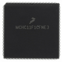
MCHC11F1CFNE3 Freescale Semiconductor, MCHC11F1CFNE3 Datasheet - Page 22

MCHC11F1CFNE3
Manufacturer Part Number
MCHC11F1CFNE3
Description
IC MCU 8BIT 1K RAM 68-PLCC
Manufacturer
Freescale Semiconductor
Series
HC11r
Specifications of MCHC11F1CFNE3
Core Processor
HC11
Core Size
8-Bit
Speed
3MHz
Connectivity
SCI, SPI
Peripherals
POR, WDT
Number Of I /o
30
Program Memory Type
ROMless
Eeprom Size
512 x 8
Ram Size
1K x 8
Voltage - Supply (vcc/vdd)
4.75 V ~ 5.25 V
Data Converters
A/D 8x8b
Oscillator Type
Internal
Operating Temperature
-40°C ~ 85°C
Package / Case
68-PLCC
A/d Inputs
8-Channel, 8-Bit
Eeprom Memory
512 Bytes
Input Output
30
Interface
SCI/SPI
Memory Type
EPROM
Number Of Bits
8
Package Type
68-pin PLCC
Programmable Memory
0 Bytes
Timers
3-16-bit
Voltage, Range
3-5.5 V
Controller Family/series
68HC11
No. Of I/o's
30
Eeprom Memory Size
512Byte
Ram Memory Size
1KB
Cpu Speed
3MHz
No. Of Timers
1
Embedded Interface Type
SCI, SPI
Rohs Compliant
Yes
Processor Series
HC11F
Core
HC11
Data Bus Width
8 bit
Program Memory Size
512 B
Data Ram Size
1 KB
Interface Type
SCI, SPI
Maximum Clock Frequency
3 MHz
Number Of Timers
1
Maximum Operating Temperature
+ 85 C
Mounting Style
SMD/SMT
Minimum Operating Temperature
- 40 C
On-chip Adc
8 bit, 8 Channel
Lead Free Status / RoHS Status
Lead free / RoHS Compliant
Program Memory Size
-
Lead Free Status / Rohs Status
RoHS Compliant part
Available stocks
Company
Part Number
Manufacturer
Quantity
Price
Company:
Part Number:
MCHC11F1CFNE3
Manufacturer:
FREESCALE
Quantity:
5 530
Company:
Part Number:
MCHC11F1CFNE3
Manufacturer:
FREESCALE
Quantity:
5 530
Company:
Part Number:
MCHC11F1CFNE3
Manufacturer:
Freescale Semiconductor
Quantity:
10 000
Company:
Part Number:
MCHC11F1CFNE3R
Manufacturer:
Freescale Semiconductor
Quantity:
10 000
2.11.2 Port B
2.11.3 Port C
2.11.4 Port D
2-8
Port B is an 8-bit output-only port. In single-chip modes, port B pins are general-pur-
pose output pins (PB[7:0]). In expanded modes, port B pins act as the high-order ad-
dress lines (ADDR[15:8]) of the address bus.
PORTB can be read at any time. Reads of PORTB return the pin driver input level. If
PORTB is written, the data is stored in internal latches. It drives the pins only in single-
chip or bootstrap mode. In expanded operating modes, port B pins are the high-order
address outputs (ADDR[15:8]).
Refer to SECTION 6 PARALLEL INPUT/OUTPUT.
Port C is an 8-bit general-purpose I/O port with a data register (PORTC) and a data
direction register (DDRC). In single-chip modes, port C pins are general-purpose I/O
pins (PC[7:0]). In expanded modes, port C pins are configured as data bus pins (DA-
TA[7:0]).
PORTC can be read at any time. Inputs return the pin level; outputs return the pin driv-
er input level. If PORTC is written, the data is stored in internal latches. It drives the
pins only if they are configured as outputs in single-chip or bootstrap mode. Port C pins
are general-purpose inputs out of reset in single-chip and bootstrap modes. In expand-
ed and test modes, these pins are data bus lines out of reset.
The CWOM control bit in the OPT2 register disables port C’s P-channel output drivers.
Because the N-channel driver is not affected by CWOM, setting CWOM causes port
C to become an open-drain-type output port suitable for wired-OR operation. In wired-
OR mode, (PORTC bits are at logic level zero), pins are actively driven low by the N-
channel driver. When a port C bit is at logic level one, the associated pin is in a high-
impedance state, as neither the N-channel nor the P-channel devices are active. It is
customary to have an external pull-up resistor on lines that are driven by open-drain
devices. Port C can only be configured for wired-OR operation when the MCU is in sin-
gle-chip or bootstrap modes.
Refer to SECTION 6 PARALLEL INPUT/OUTPUT.
Port D, a 6-bit general-purpose I/O port, has a data register (PORTD) and a data di-
rection register (DDRD). The six port D lines (D[5:0]) can be used for general-purpose
I/O, for the serial communications interface (SCI) and serial peripheral interface (SPI)
subsystems.
PORTD can be read at any time. Inputs return the pin level; outputs return the pin driv-
er input level. If PORTD is written, the data is stored in internal latches and can be driv-
en only if port D is configured for general-purpose output.
The DWOM control bit in the SPCR register disables port D’s P-channel output drivers.
Because the N-channel driver is not affected by DWOM, setting DWOM causes port
D to become an open-drain-type output port suitable for wired-OR operation. In wired-
Freescale Semiconductor, Inc.
For More Information On This Product,
Go to: www.freescale.com
PIN DESCRIPTIONS
TECHNICAL DATA
MC68HC11F1


