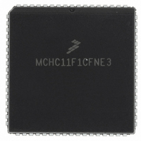
MCHC11F1CFNE3 Freescale Semiconductor, MCHC11F1CFNE3 Datasheet - Page 68

MCHC11F1CFNE3
Manufacturer Part Number
MCHC11F1CFNE3
Description
IC MCU 8BIT 1K RAM 68-PLCC
Manufacturer
Freescale Semiconductor
Series
HC11r
Specifications of MCHC11F1CFNE3
Core Processor
HC11
Core Size
8-Bit
Speed
3MHz
Connectivity
SCI, SPI
Peripherals
POR, WDT
Number Of I /o
30
Program Memory Type
ROMless
Eeprom Size
512 x 8
Ram Size
1K x 8
Voltage - Supply (vcc/vdd)
4.75 V ~ 5.25 V
Data Converters
A/D 8x8b
Oscillator Type
Internal
Operating Temperature
-40°C ~ 85°C
Package / Case
68-PLCC
A/d Inputs
8-Channel, 8-Bit
Eeprom Memory
512 Bytes
Input Output
30
Interface
SCI/SPI
Memory Type
EPROM
Number Of Bits
8
Package Type
68-pin PLCC
Programmable Memory
0 Bytes
Timers
3-16-bit
Voltage, Range
3-5.5 V
Controller Family/series
68HC11
No. Of I/o's
30
Eeprom Memory Size
512Byte
Ram Memory Size
1KB
Cpu Speed
3MHz
No. Of Timers
1
Embedded Interface Type
SCI, SPI
Rohs Compliant
Yes
Processor Series
HC11F
Core
HC11
Data Bus Width
8 bit
Program Memory Size
512 B
Data Ram Size
1 KB
Interface Type
SCI, SPI
Maximum Clock Frequency
3 MHz
Number Of Timers
1
Maximum Operating Temperature
+ 85 C
Mounting Style
SMD/SMT
Minimum Operating Temperature
- 40 C
On-chip Adc
8 bit, 8 Channel
Lead Free Status / RoHS Status
Lead free / RoHS Compliant
Program Memory Size
-
Lead Free Status / Rohs Status
RoHS Compliant part
Available stocks
Company
Part Number
Manufacturer
Quantity
Price
Company:
Part Number:
MCHC11F1CFNE3
Manufacturer:
FREESCALE
Quantity:
5 530
Company:
Part Number:
MCHC11F1CFNE3
Manufacturer:
FREESCALE
Quantity:
5 530
Company:
Part Number:
MCHC11F1CFNE3
Manufacturer:
Freescale Semiconductor
Quantity:
10 000
Company:
Part Number:
MCHC11F1CFNE3R
Manufacturer:
Freescale Semiconductor
Quantity:
10 000
5.2.6 Pulse Accumulator
5.2.7 Computer Operating Properly (COP)
5.2.8 Serial Communications Interface (SCI)
5.2.9 Serial Peripheral Interface (SPI)
5.2.10 Analog-to-Digital Converter
5.2.11 System
5.3 Reset and Interrupt Priority
5-6
The pulse accumulator system is disabled at reset so that the pulse accumulator input
(PAI) pin defaults to being a general-purpose input pin.
The COP watchdog system is enabled if the NOCOP control bit in the CONFIG regis-
ter is cleared, and disabled if NOCOP is set. The COP rate is set for the shortest du-
ration time-out.
The reset condition of the SCI system is independent of the operating mode. All trans-
mit and receive interrupts are masked and both the transmitter and receiver are dis-
abled so the port pins default to being general-purpose I/O lines. The SCI frame format
is initialized to an 8-bit character size. The send break and receiver wakeup functions
are disabled. The TDRE and TC status bits in the SCI status register are both set, in-
dicating that there is no transmit data in either the transmit data register or the transmit
serial shift register. The RDRF, IDLE, OR, NF, FE, PF, and RAF receive-related status
bits are cleared.
The SPI system is disabled by reset. The port pins associated with this function default
to being general-purpose I/O lines.
The A/D converter configuration is indeterminate after reset. The ADPU bit is cleared
by reset, which disables the A/D system. The conversion complete flag is cleared by
reset.
The EEPROM programming controls are disabled, so the memory system is config-
ured for normal read operation. PSEL[3:0] are initialized with the binary value %0101,
causing the external IRQ pin to have the highest I-bit interrupt priority. The IRQ pin is
configured for level-sensitive operation (for wired-OR systems). The RBOOT, SMOD,
and MDA bits in the HPRIO register reflect the status of the MODB and MODA inputs
at the rising edge of reset. The DLY control bit is set to specify that an oscillator start-
up delay is imposed upon recovery from STOP mode. The clock monitor system is dis-
abled because CME and FCME are cleared.
Resets and interrupts have a hardware priority that determines which reset or interrupt
is serviced first when simultaneous requests occur. Any maskable interrupt can be giv-
en priority over other maskable interrupts.
The first six interrupt sources are not maskable. The priority arrangement for these
sources is as follows:
Freescale Semiconductor, Inc.
For More Information On This Product,
RESETS AND INTERRUPTS
Go to: www.freescale.com
TECHNICAL DATA
MC68HC11F1


