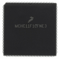
MCHC11F1CFNE3 Freescale Semiconductor, MCHC11F1CFNE3 Datasheet - Page 59

MCHC11F1CFNE3
Manufacturer Part Number
MCHC11F1CFNE3
Description
IC MCU 8BIT 1K RAM 68-PLCC
Manufacturer
Freescale Semiconductor
Series
HC11r
Specifications of MCHC11F1CFNE3
Core Processor
HC11
Core Size
8-Bit
Speed
3MHz
Connectivity
SCI, SPI
Peripherals
POR, WDT
Number Of I /o
30
Program Memory Type
ROMless
Eeprom Size
512 x 8
Ram Size
1K x 8
Voltage - Supply (vcc/vdd)
4.75 V ~ 5.25 V
Data Converters
A/D 8x8b
Oscillator Type
Internal
Operating Temperature
-40°C ~ 85°C
Package / Case
68-PLCC
A/d Inputs
8-Channel, 8-Bit
Eeprom Memory
512 Bytes
Input Output
30
Interface
SCI/SPI
Memory Type
EPROM
Number Of Bits
8
Package Type
68-pin PLCC
Programmable Memory
0 Bytes
Timers
3-16-bit
Voltage, Range
3-5.5 V
Controller Family/series
68HC11
No. Of I/o's
30
Eeprom Memory Size
512Byte
Ram Memory Size
1KB
Cpu Speed
3MHz
No. Of Timers
1
Embedded Interface Type
SCI, SPI
Rohs Compliant
Yes
Processor Series
HC11F
Core
HC11
Data Bus Width
8 bit
Program Memory Size
512 B
Data Ram Size
1 KB
Interface Type
SCI, SPI
Maximum Clock Frequency
3 MHz
Number Of Timers
1
Maximum Operating Temperature
+ 85 C
Mounting Style
SMD/SMT
Minimum Operating Temperature
- 40 C
On-chip Adc
8 bit, 8 Channel
Lead Free Status / RoHS Status
Lead free / RoHS Compliant
Program Memory Size
-
Lead Free Status / Rohs Status
RoHS Compliant part
Available stocks
Company
Part Number
Manufacturer
Quantity
Price
Company:
Part Number:
MCHC11F1CFNE3
Manufacturer:
FREESCALE
Quantity:
5 530
Company:
Part Number:
MCHC11F1CFNE3
Manufacturer:
FREESCALE
Quantity:
5 530
Company:
Part Number:
MCHC11F1CFNE3
Manufacturer:
Freescale Semiconductor
Quantity:
10 000
Company:
Part Number:
MCHC11F1CFNE3R
Manufacturer:
Freescale Semiconductor
Quantity:
10 000
CSCTL — Chip Select Control
IO1EN — I/O Chip Select 1 Enable
IO1PL — I/O Chip Select 1 Polarity Select
IO2EN — I/O Chip Select 2 Enable
IO2PL — I/O Chip Select 2 Polarity Select
GCSPR — General-Purpose Chip Select Priority
PCSEN — Program Chip Select Enable
PSIZA, PSIZB — Program Chip Select Size (A or B)
CSGADR — General-Purpose Chip Select Address Register
GA[15:10] — General-Purpose Chip Select Base Address
TECHNICAL DATA
RESET:
RESET:
*PCSEN is set out of reset in expanded modes and cleared in single-chip modes.
This bit is set out of reset in expanded modes and cleared in single-chip modes.
GA[15:10] correspond to MCU address bits ADDR[15:10] and select the starting ad-
dress of the general-purpose chip select's address range. Which bits are valid de-
pends upon the size selected by GSIZA–GSIZC in CSGSIZ register. Refer to the
following table and to Figure 4-4.
0 = CSIO1 is disabled and port G bit 5 is general-purpose I/O.
1 = CSIO1 is enabled and uses port G bit 5.
0 = CSIO1 active low
1 = CSIO1 active high
0 = CSIO2 is disabled and port G bit 4 is general-purpose I/O.
1 = CSIO2 is enabled and uses port G bit 4.
0 = CSIO2 active low
1 = CSIO2 active high
0 = Program chip select has priority over general-purpose chip select
1 = General-purpose chip select has priority over program chip select
0 = CSPROG disabled and port G bit 7 available as general-purpose I/O
1 = CSPROG enabled out of reset and uses port G bit 7 pin
IO1EN
GA15
Bit 7
Bit 7
0
0
IO1PL
PSIZA
GA14
Table 4-9 Program Chip Select Size Control
6
0
0
0
1
1
6
0
Freescale Semiconductor, Inc.
OPERATING MODES AND ON-CHIP MEMORY
For More Information On This Product,
IO2EN
GA13
5
0
5
0
Go to: www.freescale.com
PSIZB
0
1
0
1
IO2PL
GA12
4
0
4
0
Size (Bytes)
GCSPR
GA11
64 K
32 K
16 K
0
3
3
0
8 K
PCSEN*
GA10
—
2
2
0
Address Range
$C000–$FFFF
$E000–$FFFF
$0000–$FFFF
$8000–$FFFF
PSIZA
—
1
0
1
0
PSIZB
Bit 0
Bit 0
—
0
0
$105D
$105E
4-21


