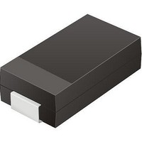
TV04A640JB-G Comchip Technology, TV04A640JB-G Datasheet - Page 13

TV04A640JB-G
Manufacturer Part Number
TV04A640JB-G
Description
TVS 400W 64V BIDIRECT SMA
Manufacturer
Comchip Technology
Specifications of TV04A640JB-G
Voltage - Reverse Standoff (typ)
64V
Voltage - Breakdown
71.1V
Power (watts)
400W
Polarization
Bidirectional
Mounting Type
Surface Mount
Package / Case
DO-214AC, SMA
Channels
1 Channel
Clamping Voltage
103 V
Operating Voltage
3.5 V
Breakdown Voltage
71.1 V
Peak Surge Current
40 A
Peak Pulse Power Dissipation
400 W
Lead Free Status / RoHS Status
Lead free / RoHS Compliant
September 8, 2009 S25FL128P_00_08
BP3
0
0
0
0
0
0
0
0
1
1
1
1
1
1
1
1
Block Protect Bits
Status Register
BP2
0
0
0
0
1
1
1
1
0
0
0
0
1
1
1
1
BP1
BP2
Software Protected Mode (SPM): The Block Protect (BP2, BP1, BP0 for uniform 256 KB sector product:
BP3, BP2, BP1, BP0 for uniform 64 KB sector product) bits define the section of the memory array that can
be read but not programmed or erased.
that are defined by Status Register bits BP2:BP0 for uniform 256 KB sector product, BP3:BP0 for uniform
64 KB sector product).
Hardware Protected Mode (HPM): The Write Protect (WP#/ACC) input and the Status Register Write
Disable (SRWD) bit together provide write protection.
Clock Pulse Count: The device verifies that all program, erase, and Write Status Register commands
consist of a clock pulse count that is a multiple of eight before executing them.
0
0
1
1
0
0
1
1
0
0
1
1
0
0
1
1
0
0
0
0
1
1
1
1
– Sector Erase (SE)
– Bulk Erase (BE)
– Write Disable (WRDI)
– Write Status Register (WRSR)
Block Protect Bits
Status Register
BP1
BP0
Table 7.2 S25FL128P Protected Area Sizes (Uniform 64 KB sector)
0
0
1
1
0
0
1
1
0
1
0
1
0
1
0
1
0
1
0
1
0
1
0
1
BP0
FE0000h-FFFFFFh
FC0000h-FFFFFFh
E00000h-FFFFFFh
C00000h-FFFFFFh
0
1
0
1
0
1
0
1
F80000h-FFFFFFh
F00000h-FFFFFFh
800000h-FFFFFFh
000000h-FFFFFFh
000000h-FFFFFFh
000000h-FFFFFFh
000000h-FFFFFFh
000000h-FFFFFFh
000000h-FFFFFFh
000000h-FFFFFFh
000000h-FFFFFFh
Table 7.1 S25FL128P Protected Area Sizes (Uniform 256 KB sector)
Address Range
Protected
None
D a t a
FC0000h-FFFFFFh
F80000h-FFFFFFh
F00000h-FFFFFFh
E00000h-FFFFFFh
C00000h-FFFFFFh
800000h-FFFFFFh
000000h-FFFFFFh
Address Range
Protected
None
S h e e t
(128) SA255:SA128
Protected Sectors
(16) SA255:SA240
(32) SA255:SA224
(64) SA255:SA192
S25FL128P
(2) SA255:SA254
(4) SA255:SA252
(8) SA255:SA248
(256) SA255:SA0
(256) SA255:SA0
(256) SA255:SA0
(256) SA255:SA0
(256) SA255:SA0
(256) SA255:SA0
(256) SA255:SA0
(256) SA255:SA0
Table 7.1
Protected Sectors
(16) SA63:SA48
(32) SA63:SA32
(0)
(2) SA63:SA62
(4) SA63:SA60
(8) SA63:SA56
(64) SA63:SA0
(1) SA63
Memory Array
(0)
shows the sizes and address ranges of protected areas
Memory Array
000000h-FFFFFFh
000000h-FDFFFFh
000000h-FBFFFFh
000000h-EFFFFFh
000000h-DFFFFFh
000000h-BFFFFFh
000000h-F7FFFFh
000000h-7FFFFFh
Address Range
Unprotected
000000h-DFFFFFh
000000h-FFFFFFh
000000h-FBFFFFh
000000h-F7FFFFh
000000h-EFFFFFh
000000h-BFFFFFh
000000h-7FFFFFh
Address Range
None
None
None
None
None
None
None
None
Unprotected
None
(256) SA255:SA0
(128) SA253:SA0
(64) SA251:SA0
(32) SA247:SA0
(16) SA239:SA0
(8) SA223:SA0
(4) SA191:SA0
(2) SA127:SA0
Unprotected
(64) SA63:SA0
(32) SA62:SA0
(16) SA61:SA0
(8) SA59:SA0
(4) SA55:SA0
(2) SA47:SA0
(1) SA31:SA0
Unprotected
Sectors
Sectors
(0)
(0)
(0)
(0)
(0)
(0)
(0)
(0)
(0)
Total Memory
Total Memory
Portion of
Protected
Protected
Portion of
1/128
Area
1/64
1/32
1/16
Area
1/64
1/32
1/16
1/8
1/4
1/2
All
All
All
All
All
All
All
All
1/4
1/8
1/2
0
All
0
13


