TV04A640JB-G Comchip Technology, TV04A640JB-G Datasheet - Page 22
TV04A640JB-G
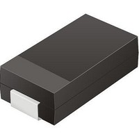
Manufacturer Part Number
TV04A640JB-G
Description
TVS 400W 64V BIDIRECT SMA
Manufacturer
Comchip Technology
Specifications of TV04A640JB-G
Voltage - Reverse Standoff (typ)
64V
Voltage - Breakdown
71.1V
Power (watts)
400W
Polarization
Bidirectional
Mounting Type
Surface Mount
Package / Case
DO-214AC, SMA
Channels
1 Channel
Clamping Voltage
103 V
Operating Voltage
3.5 V
Breakdown Voltage
71.1 V
Peak Surge Current
40 A
Peak Pulse Power Dissipation
400 W
Lead Free Status / RoHS Status
Lead free / RoHS Compliant


11.3
22
11.3.1
Read Identification (RDID: 9Fh)
Serial Mode
The Read Identification (RDID) instruction opcode allows the 8-bit manufacturer identification to be read,
follow by two bytes of device identification. The manufacturer identification is assigned by JEDEC. The device
identification is assigned by the device manufacturer.
Any Read Identification (RDID) instruction opcode issued while a program, erase, or write cycle is in progress
is not decoded and has no effect on execution of the program, erase, or write cycle that is in progress.
The device is first selected by driving the CS# chip select input pin to the logic low state. After this, the RDID
8-bit instruction opcode is shifted in onto the SI serial input pin. After the last bit of the RDID instruction
opcode is shifted into the device, a byte of manufacturer identification, two bytes of device identification and
two bytes of extended device identification will be shifted sequentially out of the SO serial output pin. Each bit
is shifted out during the falling edge of the SCK serial clock signal. The maximum clock frequency for the
RDID (9Fh) command is at 40 MHz (Normal Read).
The Read Identification (RDID) instruction sequence is terminated by driving the CS# chip select input pin to
the logic high state anytime during data output. After issuing any Read ID instruction opcodes (90h, 9Fh,
ABh), driving the CS# chip select input pin to the logic high state will automatically send the device into the
standby mode. Driving the CS# chip select input pin to the logic low state again will automatically send the
device out of the standby mode and into the active mode.
SCK
CS#
SO
SI
Figure 11.4 Read Identification Command Sequence and Data Out Sequence
0
High Impedance
1
2
Instruction
3
4
5
S25FL128P
6
D a t a
7
MSB
23
Manufacturer / Device Identification
8
22
9
S h e e t
21
10
3
28
2
29
1
30
S25FL128P_00_08 September 8, 2009
0
31
MSB
15
32
Extended Device Identification
14
33
13
34
3
44
2
45
1
46
0
47
Related parts for TV04A640JB-G
Image
Part Number
Description
Manufacturer
Datasheet
Request
R

Part Number:
Description:
Manufacturer:
Comchip Technology Corporation
Datasheet:
Part Number:
Description:
Manufacturer:
Comchip Technology Corporation
Datasheet:
Part Number:
Description:
Manufacturer:
Comchip Technology Corporation
Datasheet:
Part Number:
Description:
Manufacturer:
Comchip Technology Corporation
Datasheet:
Part Number:
Description:
Manufacturer:
Comchip Technology Corporation
Datasheet:
Part Number:
Description:
Manufacturer:
Comchip Technology Corporation
Datasheet:
Part Number:
Description:
Manufacturer:
Comchip Technology Corporation
Datasheet:
Part Number:
Description:
Manufacturer:
Comchip Technology Corporation
Datasheet:
Part Number:
Description:
Manufacturer:
Comchip Technology Corporation
Datasheet:
Part Number:
Description:
Manufacturer:
Comchip Technology Corporation
Datasheet:
Part Number:
Description:
Manufacturer:
Comchip Technology Corporation
Datasheet:
Part Number:
Description:
Manufacturer:
Comchip Technology Corporation
Datasheet:
Part Number:
Description:
Manufacturer:
Comchip Technology Corporation
Datasheet:
Part Number:
Description:
Manufacturer:
Comchip Technology Corporation
Datasheet:
Part Number:
Description:
Manufacturer:
Comchip Technology Corporation
Datasheet: