TV04A640JB-G Comchip Technology, TV04A640JB-G Datasheet - Page 9
TV04A640JB-G
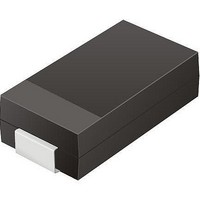
Manufacturer Part Number
TV04A640JB-G
Description
TVS 400W 64V BIDIRECT SMA
Manufacturer
Comchip Technology
Specifications of TV04A640JB-G
Voltage - Reverse Standoff (typ)
64V
Voltage - Breakdown
71.1V
Power (watts)
400W
Polarization
Bidirectional
Mounting Type
Surface Mount
Package / Case
DO-214AC, SMA
Channels
1 Channel
Clamping Voltage
103 V
Operating Voltage
3.5 V
Breakdown Voltage
71.1 V
Peak Surge Current
40 A
Peak Pulse Power Dissipation
400 W
Lead Free Status / RoHS Status
Lead free / RoHS Compliant


3. Input/Output Descriptions
4. Logic Symbol
September 8, 2009 S25FL128P_00_08
SO (Signal Data Output)
PO[7–0] (Parallel Data Input/Output)
SI (Serial Data Input)
SCK (Serial Clock)
CS# (Chip Select)
HOLD# (Hold)
WP#/ACC
(Write Protect/Accelerated Programming)
V
GND
CC
Signal Name
WP#/ACC
HOLD#
D a t a
SCK
CS#
SI
S h e e t
Input/Output
GND
V
S25FL128P
CC
Output
Input
Input
Input
Input
Input
Input
Input
I/O
Transfers parallel data into the device on the rising edge of SCK or out of
the device on the falling edge of SCK.
Transfers data serially into the device. Device latches commands,
addresses, and program data on SI on the rising edge of SCK.
Provides serial interface timing. Latches commands, addresses, and data
on SI on rising edge of SCK. Triggers output on SO after the falling edge
of SCK.
Places device in active power mode when driven low. Deselects device
and places SO at high impedance when high. After power-up, device
requires a falling edge on CS# before any command is written. Device is
in standby mode when a program, erase, or Write Status Register
operation is not in progress.
Pauses any serial communication with the device without deselecting it.
When driven low, SO is at high impedance, and all input at SI and SCK
are ignored. Requires that CS# also be driven low.
When driven low, prevents any program or erase command from altering
the data in the protected memory area specified by Status Register bits
(BP bits). If the system asserts V
programming operation is provided.
Supply Voltage
Ground
Transfers data serially out of the device on the falling edge of SCK.
SO
PO[7-0] (For 16-pin SO package)
Description
HH
on this pin, accelerated
9
Related parts for TV04A640JB-G
Image
Part Number
Description
Manufacturer
Datasheet
Request
R

Part Number:
Description:
Manufacturer:
Comchip Technology Corporation
Datasheet:
Part Number:
Description:
Manufacturer:
Comchip Technology Corporation
Datasheet:
Part Number:
Description:
Manufacturer:
Comchip Technology Corporation
Datasheet:
Part Number:
Description:
Manufacturer:
Comchip Technology Corporation
Datasheet:
Part Number:
Description:
Manufacturer:
Comchip Technology Corporation
Datasheet:
Part Number:
Description:
Manufacturer:
Comchip Technology Corporation
Datasheet:
Part Number:
Description:
Manufacturer:
Comchip Technology Corporation
Datasheet:
Part Number:
Description:
Manufacturer:
Comchip Technology Corporation
Datasheet:
Part Number:
Description:
Manufacturer:
Comchip Technology Corporation
Datasheet:
Part Number:
Description:
Manufacturer:
Comchip Technology Corporation
Datasheet:
Part Number:
Description:
Manufacturer:
Comchip Technology Corporation
Datasheet:
Part Number:
Description:
Manufacturer:
Comchip Technology Corporation
Datasheet:
Part Number:
Description:
Manufacturer:
Comchip Technology Corporation
Datasheet:
Part Number:
Description:
Manufacturer:
Comchip Technology Corporation
Datasheet:
Part Number:
Description:
Manufacturer:
Comchip Technology Corporation
Datasheet: