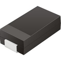
TV04A640JB-G Comchip Technology, TV04A640JB-G Datasheet - Page 21

TV04A640JB-G
Manufacturer Part Number
TV04A640JB-G
Description
TVS 400W 64V BIDIRECT SMA
Manufacturer
Comchip Technology
Specifications of TV04A640JB-G
Voltage - Reverse Standoff (typ)
64V
Voltage - Breakdown
71.1V
Power (watts)
400W
Polarization
Bidirectional
Mounting Type
Surface Mount
Package / Case
DO-214AC, SMA
Channels
1 Channel
Clamping Voltage
103 V
Operating Voltage
3.5 V
Breakdown Voltage
71.1 V
Peak Surge Current
40 A
Peak Pulse Power Dissipation
400 W
Lead Free Status / RoHS Status
Lead free / RoHS Compliant
11.2
September 8, 2009 S25FL128P_00_08
Read Data Bytes at Higher Speed (FAST_READ: 0Bh)
The FAST_READ command reads data from the memory array at the frequency (f
input, with a maximum speed of 104 MHz. The host system must first select the device by driving CS# low.
The FAST_READ command is then written to SI, followed by a 3-byte address (A23-A0) and a dummy byte.
Each bit is latched on the rising edge of SCK. The memory array data, at that address, are output serially on
SO at a frequency f
The FAST_READ command sequence is shown in
be at any location. The device automatically increments to the next higher address after each byte of data is
output. The entire memory array can therefore be read with a single FAST_READ command. When the
highest address is reached, the address counter reverts to 00000h, allowing the read sequence to continue
indefinitely.
The FAST_READ command is terminated by driving CS# high at any time during data output. The device
rejects any FAST_READ command issued while it is executing a program, erase, or Write Status Register
operation, and continues the operation uninterrupted. Note that the FAST_READ command is not valid in
parallel mode.
SCK
SO
CS#
SI
Mode 3
Mode 0
Hi-Z
Figure 11.3 Read Data Bytes at Higher Speed (FAST_READ) Command Sequence
0
1
SCK
2
Command
, on the falling edge of SCK.
3
D a t a
4
5
6
7
S h e e t
23 22 21
8
9
24-Bit Address
S25FL128P
10
28 29 30
3
2
1
Figure 11.3
31 32 33
0
7
6
Dummy Byte
34 35 36 37 38
5
and
4
3
Table
2
1
39
0
MSB
11.6. The first byte specified can
7
40 41
6
5
42 43 44 45
DATA OUT 1
SCK
4
) presented at the SCK
3
2
1
46
0
47
MSB
7
DATA OUT 2
21


