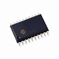
DSPIC33FJ12MC201-I/SO Microchip Technology, DSPIC33FJ12MC201-I/SO Datasheet - Page 139

DSPIC33FJ12MC201-I/SO
Manufacturer Part Number
DSPIC33FJ12MC201-I/SO
Description
IC DSPIC MCU/DSP 12K 20SOIC
Manufacturer
Microchip Technology
Series
dsPIC™ 33Fr
Datasheets
1.PIC24HJ12GP201-ISO.pdf
(84 pages)
2.DSPIC33FJ12MC201-ISO.pdf
(288 pages)
3.DSPIC33FJ12MC201-ISO.pdf
(14 pages)
4.DSPIC33FJ12MC201-IP.pdf
(284 pages)
Specifications of DSPIC33FJ12MC201-I/SO
Program Memory Type
FLASH
Program Memory Size
12KB (12K x 8)
Package / Case
20-SOIC (7.5mm Width)
Core Processor
dsPIC
Core Size
16-Bit
Speed
40 MIPs
Connectivity
I²C, IrDA, SPI, UART/USART
Peripherals
Brown-out Detect/Reset, Motor Control PWM, QEI, POR, PWM, WDT
Number Of I /o
15
Ram Size
1K x 8
Voltage - Supply (vcc/vdd)
3 V ~ 3.6 V
Data Converters
A/D 4x10b
Oscillator Type
Internal
Operating Temperature
-40°C ~ 85°C
Product
DSCs
Data Bus Width
16 bit
Processor Series
DSPIC33F
Core
dsPIC
Maximum Clock Frequency
40 MHz
Number Of Programmable I/os
15
Data Ram Size
1 KB
Maximum Operating Temperature
+ 85 C
Mounting Style
SMD/SMT
3rd Party Development Tools
52713-733, 52714-737, 53276-922, EWDSPIC
Development Tools By Supplier
PG164130, DV164035, DV244005, DV164005, PG164120, DM240001, DV164033
Minimum Operating Temperature
- 40 C
Lead Free Status / RoHS Status
Lead free / RoHS Compliant
For Use With
DV164033 - KIT START EXPLORER 16 MPLAB ICD2DM240001 - BOARD DEMO PIC24/DSPIC33/PIC32
Eeprom Size
-
Lead Free Status / Rohs Status
Lead free / RoHS Compliant
- PIC24HJ12GP201-ISO PDF datasheet
- DSPIC33FJ12MC201-ISO PDF datasheet #2
- DSPIC33FJ12MC201-ISO PDF datasheet #3
- DSPIC33FJ12MC201-IP PDF datasheet #4
- Current page: 139 of 284
- Download datasheet (5Mb)
12.0
The input capture module is useful in applications
requiring frequency (period) and pulse measurement.
The dsPIC33FJ12MC201/202 devices support up to
eight input capture channels.
The input capture module captures the 16-bit value of
the selected Time Base register when an event occurs
at the ICx pin. The events that cause a capture event
are listed below in three categories:
1.
2.
FIGURE 12-1:
© 2007 Microchip Technology Inc.
Note:
- Capture timer value on every falling edge of
- Capture timer value on every rising edge of
Note: An ‘x’ in a signal, register or bit name denotes the number of the capture channel.
Simple Capture Event modes:
input at ICx pin
input at ICx pin
Capture timer value on every edge (rising and
falling)
ICx Pin
INPUT CAPTURE
This data sheet summarizes the features
of the dsPIC33FJ12MC201/202 devices.
It is not intended to be a comprehensive
reference source. To complement the
information in this data sheet, refer to the
“dsPIC33F Family Reference Manual”.
Please see the Microchip web site
(www.microchip.com)
dsPIC33F
chapters.
Prescaler
(1, 4, 16)
Counter
3
INPUT CAPTURE BLOCK DIAGRAM
System Bus
Family
ICxCON
ICM<2:0> (ICxCON<2:0>)
ICOV, ICBNE (ICxCON<4:3>)
Mode Select
Reference
for
Edge Detection Logic
Clock Synchronizer
the
ICxI<1:0>
and
Manual
latest
Preliminary
dsPIC33FJ12MC201/202
(in IFSn Register)
Set Flag ICxIF
Interrupt
Logic
3.
Each input capture channel can select one of two
16-bit timers (Timer2 or Timer3) for the time base.
The selected timer can use either an internal or
external clock.
Other operational features include:
• Device wake-up from capture pin during CPU
• Interrupt on input capture event
• 4-word FIFO buffer for capture values
• Use of input capture to provide additional sources
- Capture timer value on every 4th rising edge
- Capture timer value on every 16th rising
Sleep and Idle modes
- Interrupt optionally generated after 1, 2, 3 or
of external interrupts
Prescaler Capture Event modes:
of input at ICx pin
edge of input at ICx pin
4 buffer locations are filled
Logic
FIFO
R/W
From 16-bit Timers
TMR2 TMR3
1
ICxBUF
16
0
DS70265B-page 137
16
ICTMR
(ICxCON<7>)
Related parts for DSPIC33FJ12MC201-I/SO
Image
Part Number
Description
Manufacturer
Datasheet
Request
R

Part Number:
Description:
IC, DSC, 16BIT, 12KB, 40MHZ, 3.6V, DIP28
Manufacturer:
Microchip Technology
Datasheet:

Part Number:
Description:
Manufacturer:
Microchip Technology Inc.
Datasheet:

Part Number:
Description:
Manufacturer:
Microchip Technology Inc.
Datasheet:

Part Number:
Description:
Manufacturer:
Microchip Technology Inc.
Datasheet:

Part Number:
Description:
Manufacturer:
Microchip Technology Inc.
Datasheet:

Part Number:
Description:
Manufacturer:
Microchip Technology Inc.
Datasheet:

Part Number:
Description:
Manufacturer:
Microchip Technology Inc.
Datasheet:

Part Number:
Description:
Manufacturer:
Microchip Technology Inc.
Datasheet:

Part Number:
Description:
Manufacturer:
Microchip Technology Inc.
Datasheet:


