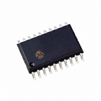
DSPIC33FJ12MC201-I/SO Microchip Technology, DSPIC33FJ12MC201-I/SO Datasheet - Page 175

DSPIC33FJ12MC201-I/SO
Manufacturer Part Number
DSPIC33FJ12MC201-I/SO
Description
IC DSPIC MCU/DSP 12K 20SOIC
Manufacturer
Microchip Technology
Series
dsPIC™ 33Fr
Datasheets
1.PIC24HJ12GP201-ISO.pdf
(84 pages)
2.DSPIC33FJ12MC201-ISO.pdf
(288 pages)
3.DSPIC33FJ12MC201-ISO.pdf
(14 pages)
4.DSPIC33FJ12MC201-IP.pdf
(284 pages)
Specifications of DSPIC33FJ12MC201-I/SO
Program Memory Type
FLASH
Program Memory Size
12KB (12K x 8)
Package / Case
20-SOIC (7.5mm Width)
Core Processor
dsPIC
Core Size
16-Bit
Speed
40 MIPs
Connectivity
I²C, IrDA, SPI, UART/USART
Peripherals
Brown-out Detect/Reset, Motor Control PWM, QEI, POR, PWM, WDT
Number Of I /o
15
Ram Size
1K x 8
Voltage - Supply (vcc/vdd)
3 V ~ 3.6 V
Data Converters
A/D 4x10b
Oscillator Type
Internal
Operating Temperature
-40°C ~ 85°C
Product
DSCs
Data Bus Width
16 bit
Processor Series
DSPIC33F
Core
dsPIC
Maximum Clock Frequency
40 MHz
Number Of Programmable I/os
15
Data Ram Size
1 KB
Maximum Operating Temperature
+ 85 C
Mounting Style
SMD/SMT
3rd Party Development Tools
52713-733, 52714-737, 53276-922, EWDSPIC
Development Tools By Supplier
PG164130, DV164035, DV244005, DV164005, PG164120, DM240001, DV164033
Minimum Operating Temperature
- 40 C
Lead Free Status / RoHS Status
Lead free / RoHS Compliant
For Use With
DV164033 - KIT START EXPLORER 16 MPLAB ICD2DM240001 - BOARD DEMO PIC24/DSPIC33/PIC32
Eeprom Size
-
Lead Free Status / Rohs Status
Lead free / RoHS Compliant
- PIC24HJ12GP201-ISO PDF datasheet
- DSPIC33FJ12MC201-ISO PDF datasheet #2
- DSPIC33FJ12MC201-ISO PDF datasheet #3
- DSPIC33FJ12MC201-IP PDF datasheet #4
- Current page: 175 of 284
- Download datasheet (5Mb)
16.0
The Serial Peripheral Interface (SPI) module is a syn-
chronous serial interface useful for communicating with
other peripheral or microcontroller devices. These
peripheral devices can be serial EEPROMs, shift regis-
ters, display drivers, analog-to-digital converters, etc.
The SPI module is compatible with SPI and SIOP from
Motorola
Each SPI module consists of a 16-bit shift register,
SPIxSR (where x = 1 or 2), used for shifting data in and
out, and a buffer register, SPIxBUF. A control register,
SPIxCON, configures the module. Additionally, a status
register, SPIxSTAT, indicates status conditions.
The serial interface consists of 4 pins:
• SDIx (serial data input)
• SDOx (serial data output)
• SCKx (shift clock input or output)
• SSx (active low slave select).
In Master mode operation, SCK is a clock output. In
Slave mode, it is a clock input.
16.1
A series of 8 or 16 clock pulses shift out bits from the
SPIxSR to SDOx pin and simultaneously shift in data
from the SDIx pin. An interrupt is generated when the
transfer is complete and the corresponding interrupt flag
bit (SPI1IF) is set. This interrupt can be disabled through
an interrupt enable bit (SPI1IE).
16.2
The receive operation is double-buffered. When a
complete byte is received, it is transferred from
SPIxSR to SPIxBUF.
If the receive buffer is full when new data is being
transferred from SPIxSR to SPIxBUF, the module sets
the SPIROV bit, indicating an overflow condition. The
transfer of the data from SPIxSR to SPIxBUF is not
completed, and the new data is lost. The module will
not respond to SCL transitions while SPIROV is ‘1’,
effectively disabling the module until SPIxBUF is read
by user software.
© 2007 Microchip Technology Inc.
Note:
®
SERIAL PERIPHERAL
INTERFACE (SPI)
Interrupts
Receive Operations
.
This data sheet summarizes the features
of the dsPIC33FJ12MC201/202 devices.
It is not intended to be a comprehensive
reference source. To complement the
information in this data sheet, refer to the
“dsPIC33F Family Reference Manual”.
Please see the Microchip web site
(www.microchip.com)
dsPIC33F
chapters.
Family
Reference
for
the
Manual
latest
Preliminary
dsPIC33FJ12MC201/202
16.3
Transmit writes are also double-buffered. The user
application writes to SPIxBUF. When the Master or
Slave transfer is completed, the contents of the shift
register (SPIxSR) are moved to the receive buffer. If any
transmit data has been written to the buffer register, the
contents of the transmit buffer are moved to SPIxSR.
The received data is thus placed in SPIxBUF and the
transmit data in SPIxSR is ready for the next transfer.
16.4
To set up the SPI module for the Master mode of
operation:
1.
2.
3.
4.
5.
Note:
If using interrupts:
a)
b)
c)
Write the desired settings to the SPIxCON
register with MSTEN (SPIxCON1<5>) = 1.
Clear the SPIROV bit (SPIxSTAT<6>).
Enable SPI operation by setting the SPIEN bit
(SPIxSTAT<15>).
Write the data to be transmitted to the SPIxBUF
register. Transmission (and reception) will start as
soon as data is written to the SPIxBUF register.
Transmit Operations
SPI Setup: Master Mode
Clear the SPIxIF bit in the respective IFSn
register.
Set the SPIxIE bit in the respective IECn
register.
Write the SPIxIP bits in the respective IPCn
register to set the interrupt priority.
Both the transmit buffer (SPIxTXB) and
the receive buffer (SPIxRXB) are mapped
to the same register address, SPIxBUF.
Do not perform read-modify-write opera-
tions (such as bit-oriented instructions) on
the SPIxBUF register.
DS70265B-page 173
Related parts for DSPIC33FJ12MC201-I/SO
Image
Part Number
Description
Manufacturer
Datasheet
Request
R

Part Number:
Description:
IC, DSC, 16BIT, 12KB, 40MHZ, 3.6V, DIP28
Manufacturer:
Microchip Technology
Datasheet:

Part Number:
Description:
Manufacturer:
Microchip Technology Inc.
Datasheet:

Part Number:
Description:
Manufacturer:
Microchip Technology Inc.
Datasheet:

Part Number:
Description:
Manufacturer:
Microchip Technology Inc.
Datasheet:

Part Number:
Description:
Manufacturer:
Microchip Technology Inc.
Datasheet:

Part Number:
Description:
Manufacturer:
Microchip Technology Inc.
Datasheet:

Part Number:
Description:
Manufacturer:
Microchip Technology Inc.
Datasheet:

Part Number:
Description:
Manufacturer:
Microchip Technology Inc.
Datasheet:

Part Number:
Description:
Manufacturer:
Microchip Technology Inc.
Datasheet:


