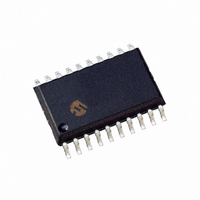
DSPIC33FJ12MC201-I/SO Microchip Technology, DSPIC33FJ12MC201-I/SO Datasheet - Page 20

DSPIC33FJ12MC201-I/SO
Manufacturer Part Number
DSPIC33FJ12MC201-I/SO
Description
IC DSPIC MCU/DSP 12K 20SOIC
Manufacturer
Microchip Technology
Series
dsPIC™ 33Fr
Datasheets
1.PIC24HJ12GP201-ISO.pdf
(84 pages)
2.DSPIC33FJ12MC201-ISO.pdf
(288 pages)
3.DSPIC33FJ12MC201-ISO.pdf
(14 pages)
4.DSPIC33FJ12MC201-IP.pdf
(284 pages)
Specifications of DSPIC33FJ12MC201-I/SO
Program Memory Type
FLASH
Program Memory Size
12KB (12K x 8)
Package / Case
20-SOIC (7.5mm Width)
Core Processor
dsPIC
Core Size
16-Bit
Speed
40 MIPs
Connectivity
I²C, IrDA, SPI, UART/USART
Peripherals
Brown-out Detect/Reset, Motor Control PWM, QEI, POR, PWM, WDT
Number Of I /o
15
Ram Size
1K x 8
Voltage - Supply (vcc/vdd)
3 V ~ 3.6 V
Data Converters
A/D 4x10b
Oscillator Type
Internal
Operating Temperature
-40°C ~ 85°C
Product
DSCs
Data Bus Width
16 bit
Processor Series
DSPIC33F
Core
dsPIC
Maximum Clock Frequency
40 MHz
Number Of Programmable I/os
15
Data Ram Size
1 KB
Maximum Operating Temperature
+ 85 C
Mounting Style
SMD/SMT
3rd Party Development Tools
52713-733, 52714-737, 53276-922, EWDSPIC
Development Tools By Supplier
PG164130, DV164035, DV244005, DV164005, PG164120, DM240001, DV164033
Minimum Operating Temperature
- 40 C
Lead Free Status / RoHS Status
Lead free / RoHS Compliant
For Use With
DV164033 - KIT START EXPLORER 16 MPLAB ICD2DM240001 - BOARD DEMO PIC24/DSPIC33/PIC32
Eeprom Size
-
Lead Free Status / Rohs Status
Lead free / RoHS Compliant
- PIC24HJ12GP201-ISO PDF datasheet
- DSPIC33FJ12MC201-ISO PDF datasheet #2
- DSPIC33FJ12MC201-ISO PDF datasheet #3
- DSPIC33FJ12MC201-IP PDF datasheet #4
- Current page: 20 of 284
- Download datasheet (5Mb)
dsPIC33FJ12MC201/202
2.5
The dsPIC33FJ12MC201/202 ALU is 16 bits wide and
is capable of addition, subtraction, bit shifts and logic
operations. Unless otherwise mentioned, arithmetic
operations are 2’s complement in nature. Depending
on the operation, the ALU can affect the values of the
Carry (C), Zero (Z), Negative (N), Overflow (OV) and
Digit Carry (DC) Status bits in the SR register. The C
and DC Status bits operate as Borrow and Digit Borrow
bits, respectively, for subtraction operations.
The ALU can perform 8-bit or 16-bit operations,
depending on the mode of the instruction that is used.
Data for the ALU operation can come from the W
register array or data memory, depending on the
addressing mode of the instruction. Likewise, output
data from the ALU can be written to the W register array
or a data memory location.
Refer to the “dsPIC30F/33F Programmer’s Reference
Manual” (DS70157) for information on the SR bits
affected by each instruction.
The dsPIC33FJ12MC201/202 CPU incorporates hard-
ware support for both multiplication and division. This
includes a dedicated hardware multiplier and support
hardware for 16-bit-divisor division.
2.5.1
Using the high-speed 17-bit x 17-bit multiplier of the
DSP engine, the ALU supports unsigned, signed or
mixed-sign operation in several MCU multiplication
modes:
• 16-bit x 16-bit signed
• 16-bit x 16-bit unsigned
• 16-bit signed x 5-bit (literal) unsigned
• 16-bit unsigned x 16-bit unsigned
• 16-bit unsigned x 5-bit (literal) unsigned
• 16-bit unsigned x 16-bit signed
• 8-bit unsigned x 8-bit unsigned
2.5.2
The divide block supports 32-bit/16-bit and 16-bit/16-bit
signed and unsigned integer divide operations with the
following data sizes:
TABLE 2-1:
DS70265B-page 18
CLR
ED
EDAC
MAC
MAC
MOVSAC
MPY
MPY
MPY.N
MSC
Arithmetic Logic Unit (ALU)
MULTIPLIER
DIVIDER
Instruction
DSP INSTRUCTIONS SUMMARY
A = 0
A = (x – y)2
A = A + (x – y)2
A = A + (x * y)
A = A + x2
No change in A
A = x * y
A = x 2
A = – x * y
A = A – x * y
Algebraic Operation
Preliminary
1.
2.
3.
4.
The quotient for all divide instructions ends up in W0
and the remainder in W1. 16-bit signed and unsigned
DIV instructions can specify any W register for both the
16-bit divisor (Wn) and any W register (aligned) pair
(W(m + 1):Wm) for the 32-bit dividend. The divide
algorithm takes one cycle per bit of divisor, so both 32-
bit/16-bit and 16-bit/16-bit instructions take the same
number of cycles to execute.
2.6
The DSP engine consists of a high-speed 17-bit x
17-bit multiplier, a barrel shifter and a 40-bit adder/
subtracter (with two target accumulators, round and
saturation logic).
The dsPIC33FJ12MC201/202 is a single-cycle instruc-
tion flow architecture; therefore, concurrent operation
of the DSP engine with MCU instruction flow is not pos-
sible. However, some MCU ALU and DSP engine
resources can be used concurrently by the same
instruction (e.g., ED, EDAC).
The DSP engine can also perform inherent accumula-
tor-to-accumulator operations that require no additional
data. These instructions are ADD, SUB and NEG.
The DSP engine has options selected through bits in
the CPU Core Control register (CORCON), as listed
below:
• Fractional or integer DSP multiply (IF)
• Signed or unsigned DSP multiply (US)
• Conventional or convergent rounding (RND)
• Automatic saturation on/off for ACCA (SATA)
• Automatic saturation on/off for ACCB (SATB)
• Automatic saturation on/off for writes to data
• Accumulator Saturation mode selection
A block diagram of the DSP engine is shown in
Figure 2-3.
memory (SATDW)
(ACCSAT)
32-bit signed/16-bit signed divide
32-bit unsigned/16-bit unsigned divide
16-bit signed/16-bit signed divide
16-bit unsigned/16-bit unsigned divide
DSP Engine
© 2007 Microchip Technology Inc.
ACC Write Back
Yes
Yes
Yes
Yes
No
No
No
No
No
No
Related parts for DSPIC33FJ12MC201-I/SO
Image
Part Number
Description
Manufacturer
Datasheet
Request
R

Part Number:
Description:
IC, DSC, 16BIT, 12KB, 40MHZ, 3.6V, DIP28
Manufacturer:
Microchip Technology
Datasheet:

Part Number:
Description:
Manufacturer:
Microchip Technology Inc.
Datasheet:

Part Number:
Description:
Manufacturer:
Microchip Technology Inc.
Datasheet:

Part Number:
Description:
Manufacturer:
Microchip Technology Inc.
Datasheet:

Part Number:
Description:
Manufacturer:
Microchip Technology Inc.
Datasheet:

Part Number:
Description:
Manufacturer:
Microchip Technology Inc.
Datasheet:

Part Number:
Description:
Manufacturer:
Microchip Technology Inc.
Datasheet:

Part Number:
Description:
Manufacturer:
Microchip Technology Inc.
Datasheet:

Part Number:
Description:
Manufacturer:
Microchip Technology Inc.
Datasheet:


