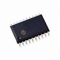
DSPIC33FJ12MC201-I/SO Microchip Technology, DSPIC33FJ12MC201-I/SO Datasheet - Page 142

DSPIC33FJ12MC201-I/SO
Manufacturer Part Number
DSPIC33FJ12MC201-I/SO
Description
IC DSPIC MCU/DSP 12K 20SOIC
Manufacturer
Microchip Technology
Series
dsPIC™ 33Fr
Datasheets
1.PIC24HJ12GP201-ISO.pdf
(84 pages)
2.DSPIC33FJ12MC201-ISO.pdf
(288 pages)
3.DSPIC33FJ12MC201-ISO.pdf
(14 pages)
4.DSPIC33FJ12MC201-IP.pdf
(284 pages)
Specifications of DSPIC33FJ12MC201-I/SO
Program Memory Type
FLASH
Program Memory Size
12KB (12K x 8)
Package / Case
20-SOIC (7.5mm Width)
Core Processor
dsPIC
Core Size
16-Bit
Speed
40 MIPs
Connectivity
I²C, IrDA, SPI, UART/USART
Peripherals
Brown-out Detect/Reset, Motor Control PWM, QEI, POR, PWM, WDT
Number Of I /o
15
Ram Size
1K x 8
Voltage - Supply (vcc/vdd)
3 V ~ 3.6 V
Data Converters
A/D 4x10b
Oscillator Type
Internal
Operating Temperature
-40°C ~ 85°C
Product
DSCs
Data Bus Width
16 bit
Processor Series
DSPIC33F
Core
dsPIC
Maximum Clock Frequency
40 MHz
Number Of Programmable I/os
15
Data Ram Size
1 KB
Maximum Operating Temperature
+ 85 C
Mounting Style
SMD/SMT
3rd Party Development Tools
52713-733, 52714-737, 53276-922, EWDSPIC
Development Tools By Supplier
PG164130, DV164035, DV244005, DV164005, PG164120, DM240001, DV164033
Minimum Operating Temperature
- 40 C
Lead Free Status / RoHS Status
Lead free / RoHS Compliant
For Use With
DV164033 - KIT START EXPLORER 16 MPLAB ICD2DM240001 - BOARD DEMO PIC24/DSPIC33/PIC32
Eeprom Size
-
Lead Free Status / Rohs Status
Lead free / RoHS Compliant
- PIC24HJ12GP201-ISO PDF datasheet
- DSPIC33FJ12MC201-ISO PDF datasheet #2
- DSPIC33FJ12MC201-ISO PDF datasheet #3
- DSPIC33FJ12MC201-IP PDF datasheet #4
- Current page: 142 of 284
- Download datasheet (5Mb)
dsPIC33FJ12MC201/202
13.3
Use the following steps when configuring the output
compare module for PWM operation:
1.
2.
3.
4.
5.
6.
13.3.1
The PWM period is specified by writing to PRy, the
Timer Period register. The PWM period can be
calculated using Equation 13-1:
EQUATION 13-2:
EXAMPLE 13-1:
DS70265B-page 140
1.
2.
Note:
Set the PWM period by writing to the selected
Timer Period register (PRy).
Set the PWM duty cycle by writing to the OCxRS
register.
Write the OxCR register with the initial duty cycle.
Enable interrupts, if required, for the timer and
output compare modules. The output compare
interrupt is required for PWM Fault pin utilization.
Configure the output compare module for one of
two PWM operation modes by writing to the
Output
(OCxCON<2:0>).
Set the TMRy prescale value and enable the
time base by setting TON = 1 (TxCON<15>).
Find the Timer Period register value for a desired PWM frequency that is 52.08 kHz, where F
prescaler setting of 1:1.
Find the maximum resolution of the duty cycle that can be used with a 52.08 kHz frequency and a 32 MHz device clock rate:
Pulse-Width Modulation Mode
T
PWM Period = 1/PWM Frequency = 1/52.08 kHz = 19.2 μs
PWM Period = (PR2 + 1) • T
19.2 μs
PR2
PWM Resolution
CY
The OCxR register should be initialized
before the output compare module is first
enabled. The OCxR register becomes a
read-only duty cycle register when the
module is operated in the PWM modes.
The value held in OCxR will become the
PWM duty cycle for the first PWM period.
The contents of the Output Compare
Secondary register, OCxRS, will not be
transferred into OCxR until a time base
period match occurs.
PWM PERIOD
Compare
CALCULATION FOR MAXIMUM PWM RESOLUTION
PWM PERIOD AND DUTY CYCLE CALCULATIONS
= 62.5 ns
= (PR2 + 1) • 62.5 ns • 1
= 306
Mode
= log
= (log
= 8.3 bits
Maximum PWM Resolution (bits) =
10
bits,
10
(F
(16 MHz/52.08 kHz)/log
CY
CY
/F
• (Timer2 Prescale Value)
OCM<2:0>
PWM
)/log
10
Preliminary
2) bits
10
2) bits
EQUATION 13-1:
13.3.2
Specify the PWM duty cycle by writing to the OCxRS reg-
ister. The OCxRS register can be written to at any time,
but the duty cycle value is not latched into OCxR until a
match between PRy and TMRy occurs (i.e., the period is
complete). This provides a double buffer for the PWM duty
cycle and is essential for glitchless PWM operation. In the
PWM mode, OCxR is a read-only register.
Some important boundary parameters of the PWM duty
cycle include:
• If the Output Compare register, OCxR, is loaded
• If OCxR is greater than PRy (Timer Period register),
• If OCxR is equal to PRy, the OCx pin will be low
See Example 13-1 for PWM mode timing details.
Tables 13-1
frequencies and resolutions for a device operating at
4, 16, and 40 MIPS.
PWM Period = [(PRy) + 1] • T
where:
PWM Frequency = 1/[PWM Period]
with 0000h, the OCx pin will remain low (0% duty
cycle).
the pin will remain high (100% duty cycle).
for one time base count value and high for all
other count values.
Note:
log
10
log
(
10
F
F
(2)
PWM
PWM DUTY CYCLE
A PRy value of N will produce a PWM
period of N + 1 time base count cycles. For
example, a value of 7 written into the PRy
register will yield a period consisting of
eight time base cycles.
CY
through 13-3
)
bits
CALCULATING THE PWM
PERIOD
© 2007 Microchip Technology Inc.
CY
CY
= 16 MHz and a Timer2
show
• (Timer Prescale Value)
example
PWM
Related parts for DSPIC33FJ12MC201-I/SO
Image
Part Number
Description
Manufacturer
Datasheet
Request
R

Part Number:
Description:
IC, DSC, 16BIT, 12KB, 40MHZ, 3.6V, DIP28
Manufacturer:
Microchip Technology
Datasheet:

Part Number:
Description:
Manufacturer:
Microchip Technology Inc.
Datasheet:

Part Number:
Description:
Manufacturer:
Microchip Technology Inc.
Datasheet:

Part Number:
Description:
Manufacturer:
Microchip Technology Inc.
Datasheet:

Part Number:
Description:
Manufacturer:
Microchip Technology Inc.
Datasheet:

Part Number:
Description:
Manufacturer:
Microchip Technology Inc.
Datasheet:

Part Number:
Description:
Manufacturer:
Microchip Technology Inc.
Datasheet:

Part Number:
Description:
Manufacturer:
Microchip Technology Inc.
Datasheet:

Part Number:
Description:
Manufacturer:
Microchip Technology Inc.
Datasheet:


