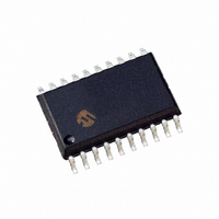
DSPIC33FJ12MC201-I/SO Microchip Technology, DSPIC33FJ12MC201-I/SO Datasheet - Page 155

DSPIC33FJ12MC201-I/SO
Manufacturer Part Number
DSPIC33FJ12MC201-I/SO
Description
IC DSPIC MCU/DSP 12K 20SOIC
Manufacturer
Microchip Technology
Series
dsPIC™ 33Fr
Datasheets
1.PIC24HJ12GP201-ISO.pdf
(84 pages)
2.DSPIC33FJ12MC201-ISO.pdf
(288 pages)
3.DSPIC33FJ12MC201-ISO.pdf
(14 pages)
4.DSPIC33FJ12MC201-IP.pdf
(284 pages)
Specifications of DSPIC33FJ12MC201-I/SO
Program Memory Type
FLASH
Program Memory Size
12KB (12K x 8)
Package / Case
20-SOIC (7.5mm Width)
Core Processor
dsPIC
Core Size
16-Bit
Speed
40 MIPs
Connectivity
I²C, IrDA, SPI, UART/USART
Peripherals
Brown-out Detect/Reset, Motor Control PWM, QEI, POR, PWM, WDT
Number Of I /o
15
Ram Size
1K x 8
Voltage - Supply (vcc/vdd)
3 V ~ 3.6 V
Data Converters
A/D 4x10b
Oscillator Type
Internal
Operating Temperature
-40°C ~ 85°C
Product
DSCs
Data Bus Width
16 bit
Processor Series
DSPIC33F
Core
dsPIC
Maximum Clock Frequency
40 MHz
Number Of Programmable I/os
15
Data Ram Size
1 KB
Maximum Operating Temperature
+ 85 C
Mounting Style
SMD/SMT
3rd Party Development Tools
52713-733, 52714-737, 53276-922, EWDSPIC
Development Tools By Supplier
PG164130, DV164035, DV244005, DV164005, PG164120, DM240001, DV164033
Minimum Operating Temperature
- 40 C
Lead Free Status / RoHS Status
Lead free / RoHS Compliant
For Use With
DV164033 - KIT START EXPLORER 16 MPLAB ICD2DM240001 - BOARD DEMO PIC24/DSPIC33/PIC32
Eeprom Size
-
Lead Free Status / Rohs Status
Lead free / RoHS Compliant
- PIC24HJ12GP201-ISO PDF datasheet
- DSPIC33FJ12MC201-ISO PDF datasheet #2
- DSPIC33FJ12MC201-ISO PDF datasheet #3
- DSPIC33FJ12MC201-IP PDF datasheet #4
- Current page: 155 of 284
- Download datasheet (5Mb)
14.16 PWM Special Event Trigger
The PWM module has a Special Event Trigger that
allows ADC conversions to be synchronized to the
PWM time base. The ADC sampling and conversion
time can be programmed to occur at any point within
the PWM period. The Special Event Trigger allows the
programmer to minimize the delay between the time
when ADC conversion results are acquired and the
time when the duty cycle value is updated.
The PWM Special Event Trigger has an SFR named
PxSECMP, and five control bits to control its operation.
The PxTMR value for which a Special Event Trigger
should occur is loaded into the PxSECMP register.
When the PWM time base is in Up/Down Count mode,
an additional control bit is required to specify the
counting phase for the Special Event Trigger. The
count phase is selected using the SEVTDIR control bit
in the PxSECMP SFR:
• If the SEVTDIR bit is cleared, the Special Event
• If the SEVTDIR bit is set, the Special Event Trig-
The SEVTDIR control bit has no effect unless the PWM
time base is configured for an Up/Down Count mode.
© 2007 Microchip Technology Inc.
Trigger occurs on the upward counting cycle of
the PWM time base.
ger occurs on the downward count cycle of the
PWM time base.
Preliminary
dsPIC33FJ12MC201/202
14.16.1
The PWM Special Event Trigger has a postscaler that
allows a 1:1 to 1:16 postscale ratio. The postscaler is
configured by writing the SEVOPS<3:0> control bits in
the PWMxCON2 SFR.
The special event output postscaler is cleared on the
following events:
• Any write to the PxSECMP register
• Any device Reset
14.17 PWM Operation During CPU Sleep
The Fault A and Fault B input pins can wake the CPU
from Sleep mode. The PWM module generates an
interrupt if either of the Fault pins is driven low while in
Sleep mode.
14.18 PWM Operation During CPU Idle
The PxTCON SFR contains a PTSIDL control bit. This
bit determines if the PWM module will continue to
operate or stop when the device enters Idle mode. If
PTSIDL = 0, the module will continue to operate. If
PTSIDL = 1, the module will stop operation as long as
the CPU remains in Idle mode.
Mode
Mode
SPECIAL EVENT TRIGGER
POSTSCALER
DS70265B-page 153
Related parts for DSPIC33FJ12MC201-I/SO
Image
Part Number
Description
Manufacturer
Datasheet
Request
R

Part Number:
Description:
IC, DSC, 16BIT, 12KB, 40MHZ, 3.6V, DIP28
Manufacturer:
Microchip Technology
Datasheet:

Part Number:
Description:
Manufacturer:
Microchip Technology Inc.
Datasheet:

Part Number:
Description:
Manufacturer:
Microchip Technology Inc.
Datasheet:

Part Number:
Description:
Manufacturer:
Microchip Technology Inc.
Datasheet:

Part Number:
Description:
Manufacturer:
Microchip Technology Inc.
Datasheet:

Part Number:
Description:
Manufacturer:
Microchip Technology Inc.
Datasheet:

Part Number:
Description:
Manufacturer:
Microchip Technology Inc.
Datasheet:

Part Number:
Description:
Manufacturer:
Microchip Technology Inc.
Datasheet:

Part Number:
Description:
Manufacturer:
Microchip Technology Inc.
Datasheet:


