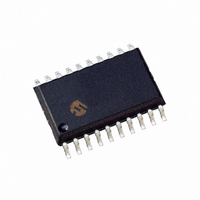
DSPIC33FJ12MC201-I/SO Microchip Technology, DSPIC33FJ12MC201-I/SO Datasheet - Page 154

DSPIC33FJ12MC201-I/SO
Manufacturer Part Number
DSPIC33FJ12MC201-I/SO
Description
IC DSPIC MCU/DSP 12K 20SOIC
Manufacturer
Microchip Technology
Series
dsPIC™ 33Fr
Datasheets
1.PIC24HJ12GP201-ISO.pdf
(84 pages)
2.DSPIC33FJ12MC201-ISO.pdf
(288 pages)
3.DSPIC33FJ12MC201-ISO.pdf
(14 pages)
4.DSPIC33FJ12MC201-IP.pdf
(284 pages)
Specifications of DSPIC33FJ12MC201-I/SO
Program Memory Type
FLASH
Program Memory Size
12KB (12K x 8)
Package / Case
20-SOIC (7.5mm Width)
Core Processor
dsPIC
Core Size
16-Bit
Speed
40 MIPs
Connectivity
I²C, IrDA, SPI, UART/USART
Peripherals
Brown-out Detect/Reset, Motor Control PWM, QEI, POR, PWM, WDT
Number Of I /o
15
Ram Size
1K x 8
Voltage - Supply (vcc/vdd)
3 V ~ 3.6 V
Data Converters
A/D 4x10b
Oscillator Type
Internal
Operating Temperature
-40°C ~ 85°C
Product
DSCs
Data Bus Width
16 bit
Processor Series
DSPIC33F
Core
dsPIC
Maximum Clock Frequency
40 MHz
Number Of Programmable I/os
15
Data Ram Size
1 KB
Maximum Operating Temperature
+ 85 C
Mounting Style
SMD/SMT
3rd Party Development Tools
52713-733, 52714-737, 53276-922, EWDSPIC
Development Tools By Supplier
PG164130, DV164035, DV244005, DV164005, PG164120, DM240001, DV164033
Minimum Operating Temperature
- 40 C
Lead Free Status / RoHS Status
Lead free / RoHS Compliant
For Use With
DV164033 - KIT START EXPLORER 16 MPLAB ICD2DM240001 - BOARD DEMO PIC24/DSPIC33/PIC32
Eeprom Size
-
Lead Free Status / Rohs Status
Lead free / RoHS Compliant
- PIC24HJ12GP201-ISO PDF datasheet
- DSPIC33FJ12MC201-ISO PDF datasheet #2
- DSPIC33FJ12MC201-ISO PDF datasheet #3
- DSPIC33FJ12MC201-IP PDF datasheet #4
- Current page: 154 of 284
- Download datasheet (5Mb)
dsPIC33FJ12MC201/202
14.14.1
The PxFLTACON SFR have four control bits that deter-
mine whether a particular pair of PWM I/O pins is to be
controlled by the Fault input pin. To enable a specific
PWM I/O pin pair for Fault overrides, the corresponding
bit should be set in the PxFLTACON register.
If all enable bits are cleared in the PxFLTACON regis-
ter, the corresponding Fault input pin has no effect on
the PWM module and the pin can be used as a general
purpose interrupt or I/O pin.
14.14.2
The PxFLTACON Special Function Registers have
eight bits each that determine the state of each PWM
I/O pin when it is overridden by a Fault input. When
these bits are cleared, the PWM I/O pin is driven to the
inactive state. If the bit is set, the PWM I/O pin is
driven to the active state. The active and inactive
states are referenced to the polarity defined for each
PWM I/O pin (HPOL and LPOL polarity control bits).
A special case exists when a PWM module I/O pair is
in the Complementary mode and both pins are
programmed to be active on a Fault condition. The
PWMxH pin always has priority in the Complementary
mode, so that both I/O pins cannot be driven active
simultaneously.
14.14.3
If both Fault input pins have been assigned to control a
particular PWM I/O pin, the Fault state programmed for
the Fault A input pin takes priority over the Fault B input
pin.
DS70265B-page 152
Note:
FAULT PIN ENABLE BITS
The Fault pin logic can operate indepen-
dent of the PWM logic. If all the enable bits
in the PxFLTACON registers are cleared,
then the Fault pin(s) could be used as gen-
eral purpose interrupt pin(s). Each Fault
pin has an interrupt vector, interrupt flag bit
and interrupt priority bits associated with it.
FAULT STATES
FAULT PIN PRIORITY
Preliminary
14.14.4
Each of the Fault input pins has two modes of
operation:
• Latched Mode: When the Fault pin is driven low,
• Cycle-by-Cycle Mode: When the Fault input pin
The operating mode for each Fault input pin is selected
using the FLTAM control bits in the PxFLTACON
Special Function Registers.
Each of the Fault pins can be controlled manually in
software.
14.15 PWM Update Lockout
For a complex PWM application, the user application
may need to write up to three Duty Cycle registers and
the PWM Time Base Period register, PxTPER, at a
given time. In some applications, it is important that all
buffer registers be written before the new duty cycle
and period values are loaded for use by the module.
The PWM update lockout feature is enabled by setting
the UDIS control bit in the PWM1CON2 SFR. The
UDIS bit affects all Duty Cycle Buffer registers and the
PWM Time Base Period register, PxTPER. No duty
cycle changes or period value changes will have effect
while UDIS = 1.
If the IUE bit is set, any change to the Duty Cycle
registers will be immediately updated regardless of the
UDIS bit state. The PWM Period register (PxTPER)
updates are not affected by the IUE control bit.
the PWM outputs go to the states defined in the
PxFLTACON registers. The PWM outputs remain
in this state until the Fault pin is driven high and
the corresponding interrupt flag has been cleared
in software. When both of these actions have
occurred, the PWM outputs return to normal oper-
ation at the beginning of the next PWM cycle or
half-cycle boundary. If the interrupt flag is cleared
before the Fault condition ends, the PWM module
waits until the Fault pin is no longer asserted to
restore the outputs.
is driven low, the PWM outputs remain in the
defined Fault states for as long as the Fault pin is
held low. After the Fault pin is driven high, the
PWM outputs return to normal operation at the
beginning of the following PWM cycle or
half-cycle boundary.
FAULT INPUT MODES
© 2007 Microchip Technology Inc.
Related parts for DSPIC33FJ12MC201-I/SO
Image
Part Number
Description
Manufacturer
Datasheet
Request
R

Part Number:
Description:
IC, DSC, 16BIT, 12KB, 40MHZ, 3.6V, DIP28
Manufacturer:
Microchip Technology
Datasheet:

Part Number:
Description:
Manufacturer:
Microchip Technology Inc.
Datasheet:

Part Number:
Description:
Manufacturer:
Microchip Technology Inc.
Datasheet:

Part Number:
Description:
Manufacturer:
Microchip Technology Inc.
Datasheet:

Part Number:
Description:
Manufacturer:
Microchip Technology Inc.
Datasheet:

Part Number:
Description:
Manufacturer:
Microchip Technology Inc.
Datasheet:

Part Number:
Description:
Manufacturer:
Microchip Technology Inc.
Datasheet:

Part Number:
Description:
Manufacturer:
Microchip Technology Inc.
Datasheet:

Part Number:
Description:
Manufacturer:
Microchip Technology Inc.
Datasheet:


