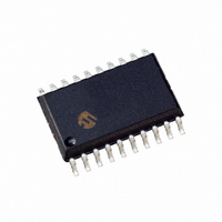
DSPIC33FJ12MC201-I/SO Microchip Technology, DSPIC33FJ12MC201-I/SO Datasheet - Page 152

DSPIC33FJ12MC201-I/SO
Manufacturer Part Number
DSPIC33FJ12MC201-I/SO
Description
IC DSPIC MCU/DSP 12K 20SOIC
Manufacturer
Microchip Technology
Series
dsPIC™ 33Fr
Datasheets
1.PIC24HJ12GP201-ISO.pdf
(84 pages)
2.DSPIC33FJ12MC201-ISO.pdf
(288 pages)
3.DSPIC33FJ12MC201-ISO.pdf
(14 pages)
4.DSPIC33FJ12MC201-IP.pdf
(284 pages)
Specifications of DSPIC33FJ12MC201-I/SO
Program Memory Type
FLASH
Program Memory Size
12KB (12K x 8)
Package / Case
20-SOIC (7.5mm Width)
Core Processor
dsPIC
Core Size
16-Bit
Speed
40 MIPs
Connectivity
I²C, IrDA, SPI, UART/USART
Peripherals
Brown-out Detect/Reset, Motor Control PWM, QEI, POR, PWM, WDT
Number Of I /o
15
Ram Size
1K x 8
Voltage - Supply (vcc/vdd)
3 V ~ 3.6 V
Data Converters
A/D 4x10b
Oscillator Type
Internal
Operating Temperature
-40°C ~ 85°C
Product
DSCs
Data Bus Width
16 bit
Processor Series
DSPIC33F
Core
dsPIC
Maximum Clock Frequency
40 MHz
Number Of Programmable I/os
15
Data Ram Size
1 KB
Maximum Operating Temperature
+ 85 C
Mounting Style
SMD/SMT
3rd Party Development Tools
52713-733, 52714-737, 53276-922, EWDSPIC
Development Tools By Supplier
PG164130, DV164035, DV244005, DV164005, PG164120, DM240001, DV164033
Minimum Operating Temperature
- 40 C
Lead Free Status / RoHS Status
Lead free / RoHS Compliant
For Use With
DV164033 - KIT START EXPLORER 16 MPLAB ICD2DM240001 - BOARD DEMO PIC24/DSPIC33/PIC32
Eeprom Size
-
Lead Free Status / Rohs Status
Lead free / RoHS Compliant
- PIC24HJ12GP201-ISO PDF datasheet
- DSPIC33FJ12MC201-ISO PDF datasheet #2
- DSPIC33FJ12MC201-ISO PDF datasheet #3
- DSPIC33FJ12MC201-IP PDF datasheet #4
- Current page: 152 of 284
- Download datasheet (5Mb)
dsPIC33FJ12MC201/202
FIGURE 14-5:
14.9.2
The PxDTCON2 SFR contains control bits that allow
the dead times to be assigned to each of the comple-
mentary outputs. Table 14-1 summarizes the function
of each dead-time selection control bit.
TABLE 14-1:
DS70265B-page 150
DTS1A Selects PWMxL1/PWMxH1 active edge
DTS1I
DTS2A Selects PWMxL2/PWMxH2 active edge
DTS2I
DTS3A Selects PWMxL3/PWMxH3 active edge
DTS3I
Bit
Duty Cycle Generator
PWMxH
PWMxL
Time Selected by DTSxA bit (A or B)
dead time.
Selects PWMxL1/PWMxH1 inactive edge
dead time.
dead time.
Selects PWMxL2/PWMxH2 inactive edge
dead time.
dead time.
Selects PWMxL3/PWMxH3 inactive edge
dead time.
DEAD-TIME ASSIGNMENT
DEAD-TIME SELECTION BITS
DEAD-TIME TIMING DIAGRAM
Function
Preliminary
14.9.3
The amount of dead time provided by each dead-time
unit is selected by specifying the input clock prescaler
value and a 6-bit unsigned value. The amount of dead
time provided by each unit can be set independently.
Four input clock prescaler selections have been pro-
vided to allow a suitable range of dead times, based on
the device operating frequency. The clock prescaler
option can be selected independently for each of the
two dead-time values. The dead-time clock prescaler
values are selected using the DTAPS<1:0> and
DTBPS<1:0> control bits in the PxDTCON1 SFR. One
of four clock prescaler options (T
T
After the prescaler values are selected, the dead time
for each unit is adjusted by loading two 6-bit unsigned
values into the PxDTCON1 SFR.
The dead-time unit prescalers are cleared on the
following events:
• On a load of the down timer due to a duty cycle
• On a write to the PxDTCON1 or PxDTCON2
• On any device Reset.
CY
comparison edge event.
registers.
Note:
) can be selected for each of the dead-time values.
DEAD-TIME RANGES
The user application should not modify the
PxDTCON1 or PxDTCON2 values while
the PWM module is operating (PTEN = 1).
Unexpected results can occur.
Time Selected by DTSxI bit (A or B)
© 2007 Microchip Technology Inc.
CY
, 2 T
CY
, 4 T
CY
or 8
Related parts for DSPIC33FJ12MC201-I/SO
Image
Part Number
Description
Manufacturer
Datasheet
Request
R

Part Number:
Description:
IC, DSC, 16BIT, 12KB, 40MHZ, 3.6V, DIP28
Manufacturer:
Microchip Technology
Datasheet:

Part Number:
Description:
Manufacturer:
Microchip Technology Inc.
Datasheet:

Part Number:
Description:
Manufacturer:
Microchip Technology Inc.
Datasheet:

Part Number:
Description:
Manufacturer:
Microchip Technology Inc.
Datasheet:

Part Number:
Description:
Manufacturer:
Microchip Technology Inc.
Datasheet:

Part Number:
Description:
Manufacturer:
Microchip Technology Inc.
Datasheet:

Part Number:
Description:
Manufacturer:
Microchip Technology Inc.
Datasheet:

Part Number:
Description:
Manufacturer:
Microchip Technology Inc.
Datasheet:

Part Number:
Description:
Manufacturer:
Microchip Technology Inc.
Datasheet:


