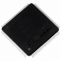
ST92F150CV1TB STMicroelectronics, ST92F150CV1TB Datasheet - Page 11

ST92F150CV1TB
Manufacturer Part Number
ST92F150CV1TB
Description
MCU 8BIT 128K FLASH 100TQFP
Manufacturer
STMicroelectronics
Series
ST9r
Datasheet
1.ST92F150CV1TB.pdf
(429 pages)
Specifications of ST92F150CV1TB
Core Processor
ST9
Core Size
8/16-Bit
Speed
24MHz
Connectivity
CAN, EBI/EMI, I²C, LIN, SCI, SPI
Peripherals
DMA, LVD, POR, PWM, WDT
Number Of I /o
77
Program Memory Size
128KB (128K x 8)
Program Memory Type
FLASH
Eeprom Size
1K x 8
Ram Size
4K x 8
Voltage - Supply (vcc/vdd)
4.5 V ~ 5.5 V
Data Converters
A/D 16x10b
Oscillator Type
Internal
Operating Temperature
-40°C ~ 105°C
Package / Case
100-TQFP, 100-VQFP
Processor Series
ST92F15x
Core
ST9
Data Bus Width
8 bit, 16 bit
Data Ram Size
6 KB
Interface Type
CAN, I2C, SCI, SPI
Maximum Clock Frequency
24 MHz
Number Of Programmable I/os
80
Number Of Timers
5 x 16 bit
Operating Supply Voltage
4.5 V to 5.5 V
Maximum Operating Temperature
+ 105 C
Mounting Style
SMD/SMT
Development Tools By Supplier
ST92F150-EPB
Minimum Operating Temperature
- 40 C
On-chip Adc
16 bit x 10 bit
Lead Free Status / RoHS Status
Lead free / RoHS Compliant
Other names
497-4883
Available stocks
Company
Part Number
Manufacturer
Quantity
Price
Company:
Part Number:
ST92F150CV1TB
Manufacturer:
STMicroelectronics
Quantity:
10 000
- Current page: 11 of 429
- Download datasheet (8Mb)
1.2 PIN DESCRIPTION
AS. Address Strobe (output, active low, 3-state).
Address Strobe is pulsed low once at the begin-
ning of each memory cycle. The rising edge of AS
indicates that address, Read/Write (RW), and
Data signals are valid for memory transfers.
DS. Data Strobe (output, active low, 3-state). Data
Strobe provides the timing for data movement to or
from Port 0 for each memory transfer. During a
write cycle, data out is valid at the leading edge of
DS. During a read cycle, Data In must be valid pri-
or to the trailing edge of DS. When the ST9 ac-
cesses on-chip memory, DS is held high during
the whole memory cycle.
RESET. Reset (input, active low). The ST9 is ini-
tialised by the Reset signal. With the deactivation
of RESET, program execution begins from the
Program memory location pointed to by the vector
contained in program memory locations 00h and
01h.
RW. Read/Write (output, 3-state). Read/Write de-
termines the direction of data transfer for external
memory transactions. RW is low when writing to
external memory, and high for all other transac-
tions.
OSCIN, OSCOUT. Oscillator (input and output).
These pins connect a parallel-resonant crystal, or
an external source to the on-chip clock oscillator
and buffer. OSCIN is the input of the oscillator in-
verter; OSCOUT is the output of the oscillator in-
verter.
HW0SW1. When connected to V
pull-up resistor, the software watchdog option is
selected. When connected to V
pull-down resistor, the hardware watchdog option
is selected.
VPWO. This pin is the output line of the J1850 pe-
ripheral (JBLPD). It is available only on some de-
vices.
RX1/WKUP6. Receive Data input of CAN1 and
Wake-up line 6. Available only on some devices.
When the CAN1 peripheral is disabled, a pull-up
resistor is connected internally to this pin.
TX1. Transmit Data output of CAN1. Available on
some devices.
SS
DD
through a 1K
through a 1K
ST92F124/F150/F250 - GENERAL DESCRIPTION
P0[7:0], P1[7:0] or P9[7:2] (Input/Output, TTL or
CMOS compatible). 11 lines (64-pin devices) or 22
lines (100-pin devices) providing the external
memory interface for addressing 2K or 4M bytes of
external memory.
P0[7:0], P1[2:0], P2[7:0], P3[7:4], P4.[7:4],
P5[7:0], P6[5:2,0], P7[7:0] I/O Port Lines (Input/
Output, TTL or CMOS compatible). I/O lines
grouped into I/O ports of 8 bits, bit programmable
under software control as general purpose I/O or
as alternate functions.
P1[7:3], P3[3:1], P4[3:0], P6.1, P8[7:0], P9[7:0]
Additional I/O Port Lines available on 100-pin ver-
sions only.
P3.0, P6[7:6] Additional I/O Port Lines available
on ST92F250 version only.
AV
verter (common for ADC 0 and ADC 1).
AVDD can be switched off when the ADC is not in
use.
AV
verter (common for ADC 0 and ADC 1).
V
available on 100-pin versions, two on 64-pin ver-
sions. The pins are internally connected.
V
ble on 100-pin versions, two on 64-pin versions.
The pins are internally connected.
V
poses. This pin must be kept to 0 in user mode.
V
age regulator. The user must connect external sta-
bilization capacitors to these pins. Refer to
16.
1.2.1 I/O Port Alternate Functions
Each pin of the I/O ports of the ST92F124/F150/
F250 may assume software programmable Alter-
nate Functions as shown in
1.2.2 Termination of Unused Pins
For unused pins, input mode is not recommended.
These pins must be kept at a fixed voltage using
the output push pull mode of the I/O or an external
pull-up or pull-down resistor.
DD
SS
TEST
REG
DD
SS
. Digital Circuit Ground. Four pins are availa-
. Main Power Supply Voltage. Four pins are
. Stabilization capacitors for the internal volt-
. Analog V
. Analog V
Power Supply Voltage for Flash test pur-
SS
DD
of the Analog to Digital Con-
of the Analog to Digital Con-
Section
1.4.
Figure
11/429
9
Related parts for ST92F150CV1TB
Image
Part Number
Description
Manufacturer
Datasheet
Request
R

Part Number:
Description:
BOARD PROGRAM FOR ST92F150 MCU
Manufacturer:
STMicroelectronics
Datasheet:

Part Number:
Description:
BOARD EVALUATION FOR ST9 SERIES
Manufacturer:
STMicroelectronics
Datasheet:

Part Number:
Description:
BOARD EMULATOR FOR ST9 SERIES
Manufacturer:
STMicroelectronics
Datasheet:

Part Number:
Description:
MCU, MPU & DSP Development Tools ST9 Dedication Board
Manufacturer:
STMicroelectronics
Datasheet:

Part Number:
Description:
STMicroelectronics [RIPPLE-CARRY BINARY COUNTER/DIVIDERS]
Manufacturer:
STMicroelectronics
Datasheet:

Part Number:
Description:
STMicroelectronics [LIQUID-CRYSTAL DISPLAY DRIVERS]
Manufacturer:
STMicroelectronics
Datasheet:

Part Number:
Description:
BOARD EVAL FOR MEMS SENSORS
Manufacturer:
STMicroelectronics
Datasheet:

Part Number:
Description:
NPN TRANSISTOR POWER MODULE
Manufacturer:
STMicroelectronics
Datasheet:

Part Number:
Description:
TURBOSWITCH ULTRA-FAST HIGH VOLTAGE DIODE
Manufacturer:
STMicroelectronics
Datasheet:

Part Number:
Description:
Manufacturer:
STMicroelectronics
Datasheet:

Part Number:
Description:
DIODE / SCR MODULE
Manufacturer:
STMicroelectronics
Datasheet:

Part Number:
Description:
DIODE / SCR MODULE
Manufacturer:
STMicroelectronics
Datasheet:


