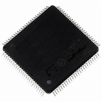
ST92F150CV1TB STMicroelectronics, ST92F150CV1TB Datasheet - Page 205

ST92F150CV1TB
Manufacturer Part Number
ST92F150CV1TB
Description
MCU 8BIT 128K FLASH 100TQFP
Manufacturer
STMicroelectronics
Series
ST9r
Datasheet
1.ST92F150CV1TB.pdf
(429 pages)
Specifications of ST92F150CV1TB
Core Processor
ST9
Core Size
8/16-Bit
Speed
24MHz
Connectivity
CAN, EBI/EMI, I²C, LIN, SCI, SPI
Peripherals
DMA, LVD, POR, PWM, WDT
Number Of I /o
77
Program Memory Size
128KB (128K x 8)
Program Memory Type
FLASH
Eeprom Size
1K x 8
Ram Size
4K x 8
Voltage - Supply (vcc/vdd)
4.5 V ~ 5.5 V
Data Converters
A/D 16x10b
Oscillator Type
Internal
Operating Temperature
-40°C ~ 105°C
Package / Case
100-TQFP, 100-VQFP
Processor Series
ST92F15x
Core
ST9
Data Bus Width
8 bit, 16 bit
Data Ram Size
6 KB
Interface Type
CAN, I2C, SCI, SPI
Maximum Clock Frequency
24 MHz
Number Of Programmable I/os
80
Number Of Timers
5 x 16 bit
Operating Supply Voltage
4.5 V to 5.5 V
Maximum Operating Temperature
+ 105 C
Mounting Style
SMD/SMT
Development Tools By Supplier
ST92F150-EPB
Minimum Operating Temperature
- 40 C
On-chip Adc
16 bit x 10 bit
Lead Free Status / RoHS Status
Lead free / RoHS Compliant
Other names
497-4883
Available stocks
Company
Part Number
Manufacturer
Quantity
Price
Company:
Part Number:
ST92F150CV1TB
Manufacturer:
STMicroelectronics
Quantity:
10 000
- Current page: 205 of 429
- Download datasheet (8Mb)
MULTIFUNCTION TIMER (Cont’d)
EXTERNAL
(T_ICR)
R250 - Read/Write
Register Page: 10
Reset value: 0000 0000 (00h)
Bits 7:4 = IN[3:0]: Input pin function.
These bits are set and cleared by software.
Bits 3:2 = A[0:1]: TxINA Pin event.
These bits are set and cleared by software.
IN3
7
IN[3:0] bits
A0
0
0
1
1
0000
0001
0010
0011
0100
0101
0110
0111
1000
1001
1010
1011
1100
1101
1110
1111
IN2
IN1
A1
INPUT
0
1
0
1
Pin Function
Trigger Up
Ext. Clock
Autodiscr.
IN0
Clock Up
Up/Down
Up/Down
not used
not used
not used
Trigger
Trigger
Trigger
Trigger
No operation
Falling edge sensitive
Rising edge sensitive
Rising and falling edges
TxINA
Gate
Gate
Gate
CONTROL
A0
TxINA Pin Event
A1
Pin Function
Trigger Down
TxINB Input
Clock Down
Ext. Clock
Ext. Clock
Ext. Clock
Ext. Clock
Autodiscr.
not used
not used
not used
not used
Trigger
Trigger
Trigger
Trigger
REGISTER
B0
Gate
B1
0
Bits 1:0 = B[0:1]: TxINB Pin event.
These bits are set and cleared by software.
PRESCALER REGISTER (PRSR)
R251 - Read/Write
Register Page: 10
Reset value: 0000 0000 (00h)
This register holds the preset value for the 8-bit
prescaler. The PRSR content may be modified at
any time, but it will be loaded into the prescaler at
the following prescaler underflow, or as a conse-
quence of a counter reload (either by software or
upon external request).
Following a RESET condition, the prescaler is au-
tomatically loaded with 00h, so that the prescaler
divides by 1 and the maximum counter clock is
generated (Crystal oscillator clock frequency divid-
ed by 6 when MODER.5 = DIV2 bit is set).
The binary value programmed in the PRSR regis-
ter is equal to the divider value minus one. For ex-
ample, loading PRSR with 24 causes the prescal-
er to divide by 25.
P7
7
B0
0
0
1
1
P6
MULTIFUNCTION TIMER (MFT)
B1
P5
0
1
0
1
P4
No operation
Falling edge sensitive
Rising edge sensitive
Rising and falling edges
P3
TxINB Pin Event
P2
P1
205/429
P0
0
9
Related parts for ST92F150CV1TB
Image
Part Number
Description
Manufacturer
Datasheet
Request
R

Part Number:
Description:
BOARD PROGRAM FOR ST92F150 MCU
Manufacturer:
STMicroelectronics
Datasheet:

Part Number:
Description:
BOARD EVALUATION FOR ST9 SERIES
Manufacturer:
STMicroelectronics
Datasheet:

Part Number:
Description:
BOARD EMULATOR FOR ST9 SERIES
Manufacturer:
STMicroelectronics
Datasheet:

Part Number:
Description:
MCU, MPU & DSP Development Tools ST9 Dedication Board
Manufacturer:
STMicroelectronics
Datasheet:

Part Number:
Description:
STMicroelectronics [RIPPLE-CARRY BINARY COUNTER/DIVIDERS]
Manufacturer:
STMicroelectronics
Datasheet:

Part Number:
Description:
STMicroelectronics [LIQUID-CRYSTAL DISPLAY DRIVERS]
Manufacturer:
STMicroelectronics
Datasheet:

Part Number:
Description:
BOARD EVAL FOR MEMS SENSORS
Manufacturer:
STMicroelectronics
Datasheet:

Part Number:
Description:
NPN TRANSISTOR POWER MODULE
Manufacturer:
STMicroelectronics
Datasheet:

Part Number:
Description:
TURBOSWITCH ULTRA-FAST HIGH VOLTAGE DIODE
Manufacturer:
STMicroelectronics
Datasheet:

Part Number:
Description:
Manufacturer:
STMicroelectronics
Datasheet:

Part Number:
Description:
DIODE / SCR MODULE
Manufacturer:
STMicroelectronics
Datasheet:

Part Number:
Description:
DIODE / SCR MODULE
Manufacturer:
STMicroelectronics
Datasheet:


