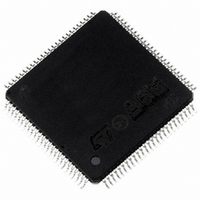
ST92F150CV1TB STMicroelectronics, ST92F150CV1TB Datasheet - Page 415

ST92F150CV1TB
Manufacturer Part Number
ST92F150CV1TB
Description
MCU 8BIT 128K FLASH 100TQFP
Manufacturer
STMicroelectronics
Series
ST9r
Datasheet
1.ST92F150CV1TB.pdf
(429 pages)
Specifications of ST92F150CV1TB
Core Processor
ST9
Core Size
8/16-Bit
Speed
24MHz
Connectivity
CAN, EBI/EMI, I²C, LIN, SCI, SPI
Peripherals
DMA, LVD, POR, PWM, WDT
Number Of I /o
77
Program Memory Size
128KB (128K x 8)
Program Memory Type
FLASH
Eeprom Size
1K x 8
Ram Size
4K x 8
Voltage - Supply (vcc/vdd)
4.5 V ~ 5.5 V
Data Converters
A/D 16x10b
Oscillator Type
Internal
Operating Temperature
-40°C ~ 105°C
Package / Case
100-TQFP, 100-VQFP
Processor Series
ST92F15x
Core
ST9
Data Bus Width
8 bit, 16 bit
Data Ram Size
6 KB
Interface Type
CAN, I2C, SCI, SPI
Maximum Clock Frequency
24 MHz
Number Of Programmable I/os
80
Number Of Timers
5 x 16 bit
Operating Supply Voltage
4.5 V to 5.5 V
Maximum Operating Temperature
+ 105 C
Mounting Style
SMD/SMT
Development Tools By Supplier
ST92F150-EPB
Minimum Operating Temperature
- 40 C
On-chip Adc
16 bit x 10 bit
Lead Free Status / RoHS Status
Lead free / RoHS Compliant
Other names
497-4883
Available stocks
Company
Part Number
Manufacturer
Quantity
Price
Company:
Part Number:
ST92F150CV1TB
Manufacturer:
STMicroelectronics
Quantity:
10 000
- Current page: 415 of 429
- Download datasheet (8Mb)
KNOWN LIMITATIONS (Cont’d)
Workaround 1
The workaround is to replace any occurrence of
by
x=0 for the CAN_0 cell
x=1 for the CAN_1 cell
y=0 for the Receive FIFO 0
y=1 for the Receive FIFO 1
Explanation of Workaround 1
First, we need to make sure no interrupt can occur
between the test and the release of the FIFO to
avoid any added delay.
The workaround checks if the first 2 FIFO levels
are already full (FMP = 2) as the problem happens
only in this case.
If FMP≠2 we release the FIFO immediately, if
FMP=2, we monitor the reception status of the
cell.
The reception status is available in the CMSR reg-
ister bit 5 (REC bit).
Note: The REC bit was called RX in olders ver-
sions of the datasheet.
If the cell is not receiving, then REC bit in CMSR is
at 0, the software can release the FIFO immedi-
ately: there is no risk.
If the cell is receiving, it is important to make sure
the release of the mailbox will not happen at the
spp (CANx_CTRL_PG);
CANx_CTRL_CRFRy |= CRFR_rfom;
spp(CANx_CTRL_PG);
if ((CANx_CTRL_CRFRy & 0x03) == 0x02)
while (( CANx_CTRL_CMSRy & 0x20) && (CANx_CTRL_CDGRy & 0x08));
CANx_CTRL_CRFRy |= CRFR_rfom;
:
ST92F124/F150/F250 - KNOWN LIMITATIONS
:
time when the received message is loaded into the
FIFO.
We could simply wait for the end of the reception,
but this could take a long time (200µs for a 100-bit
frame at 500kHz), so we also monitor the Rx pin of
the microcontroller to minimize the time the appli-
cation may wait in the while loop.
We know the critical window is located at the end
of the frame, 6+ CAN bit times after the acknowl-
edge bit (exactly six full bit times plus the time from
the beginning of the bit to the sample point). Those
bits represent the acknowledge delimiter + the end
of frame slot.
We know also that those 6+ bits are in recessive
state on the bus, therefore if the CAN Rx pin of the
device is at ‘0’, (reflecting a CAN dominant state
on the bus), this is early enough to be sure we can
release the FIFO before the critical time slot.
Therefore, if the device hardware pin Rx is at 0
and there is a reception on going, its message will
be transferred to the FIFO only 6+ CAN bit times
later at the earliest (if the dominant bit is the ac-
knowledge) or later if the dominant bit is part of the
message.
415/429
1
Related parts for ST92F150CV1TB
Image
Part Number
Description
Manufacturer
Datasheet
Request
R

Part Number:
Description:
BOARD PROGRAM FOR ST92F150 MCU
Manufacturer:
STMicroelectronics
Datasheet:

Part Number:
Description:
BOARD EVALUATION FOR ST9 SERIES
Manufacturer:
STMicroelectronics
Datasheet:

Part Number:
Description:
BOARD EMULATOR FOR ST9 SERIES
Manufacturer:
STMicroelectronics
Datasheet:

Part Number:
Description:
MCU, MPU & DSP Development Tools ST9 Dedication Board
Manufacturer:
STMicroelectronics
Datasheet:

Part Number:
Description:
STMicroelectronics [RIPPLE-CARRY BINARY COUNTER/DIVIDERS]
Manufacturer:
STMicroelectronics
Datasheet:

Part Number:
Description:
STMicroelectronics [LIQUID-CRYSTAL DISPLAY DRIVERS]
Manufacturer:
STMicroelectronics
Datasheet:

Part Number:
Description:
BOARD EVAL FOR MEMS SENSORS
Manufacturer:
STMicroelectronics
Datasheet:

Part Number:
Description:
NPN TRANSISTOR POWER MODULE
Manufacturer:
STMicroelectronics
Datasheet:

Part Number:
Description:
TURBOSWITCH ULTRA-FAST HIGH VOLTAGE DIODE
Manufacturer:
STMicroelectronics
Datasheet:

Part Number:
Description:
Manufacturer:
STMicroelectronics
Datasheet:

Part Number:
Description:
DIODE / SCR MODULE
Manufacturer:
STMicroelectronics
Datasheet:

Part Number:
Description:
DIODE / SCR MODULE
Manufacturer:
STMicroelectronics
Datasheet:


