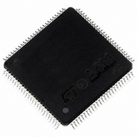
ST92F150CV1TB STMicroelectronics, ST92F150CV1TB Datasheet - Page 60

ST92F150CV1TB
Manufacturer Part Number
ST92F150CV1TB
Description
MCU 8BIT 128K FLASH 100TQFP
Manufacturer
STMicroelectronics
Series
ST9r
Datasheet
1.ST92F150CV1TB.pdf
(429 pages)
Specifications of ST92F150CV1TB
Core Processor
ST9
Core Size
8/16-Bit
Speed
24MHz
Connectivity
CAN, EBI/EMI, I²C, LIN, SCI, SPI
Peripherals
DMA, LVD, POR, PWM, WDT
Number Of I /o
77
Program Memory Size
128KB (128K x 8)
Program Memory Type
FLASH
Eeprom Size
1K x 8
Ram Size
4K x 8
Voltage - Supply (vcc/vdd)
4.5 V ~ 5.5 V
Data Converters
A/D 16x10b
Oscillator Type
Internal
Operating Temperature
-40°C ~ 105°C
Package / Case
100-TQFP, 100-VQFP
Processor Series
ST92F15x
Core
ST9
Data Bus Width
8 bit, 16 bit
Data Ram Size
6 KB
Interface Type
CAN, I2C, SCI, SPI
Maximum Clock Frequency
24 MHz
Number Of Programmable I/os
80
Number Of Timers
5 x 16 bit
Operating Supply Voltage
4.5 V to 5.5 V
Maximum Operating Temperature
+ 105 C
Mounting Style
SMD/SMT
Development Tools By Supplier
ST92F150-EPB
Minimum Operating Temperature
- 40 C
On-chip Adc
16 bit x 10 bit
Lead Free Status / RoHS Status
Lead free / RoHS Compliant
Other names
497-4883
Available stocks
Company
Part Number
Manufacturer
Quantity
Price
Company:
Part Number:
ST92F150CV1TB
Manufacturer:
STMicroelectronics
Quantity:
10 000
- Current page: 60 of 429
- Download datasheet (8Mb)
ST92F124/F150/F250 - SINGLE VOLTAGE FLASH & E3 TM (EMULATED EEPROM)
3.4 WRITE OPERATION EXAMPLE
Each operation (both Flash and
by a sequence of instructions like the following:
OR
LD
LD
..
LD
OR
The first instruction is used to select the desired
operation by setting its corresponding selection bit
in the Control Register (FCR for Flash operations,
ECR for
Table 11. Flash Write Operations
Table 12.
60/429
9
Sector Erase Suspend
FCR, #OPMASK ;Operation selection
ADD1, #DATA1 ;1st Add and Data
ADD2, #DATA2 ;2nd Add and Data
...., ......
ADDn, #DATAn ;nth Add and Data
FCR, #80h
Page Program
Set Protection
Byte Program
Sector Erase
Page Update
Chip Erase
Chip Erase
E
Operation
Operation
3 TM
E
3 TM
operations).
Write Operations
;n range = (1 to 16)
;Operation start
Selection bit
Selection bit
FPAGE
EPAGE
E
FSECT
FSUSP
FBYTE
FCHIP
ECHIP
PROT
3 TM
) is activated
Addresses and Data
Addresses and Data
From 1 to 4 sectors
From 1 to 16 bytes
From 1 to 16 bytes
From 1 to 4 bytes
The load instructions are used to set the address-
es (in the Flash or in the
the data to be modified.
The last instruction is used to start the write oper-
ation, by setting the start bit (FWMS for Flash op-
erations, EWMS for
register.
Once selected, but not yet started, one operation
can be cancelled by resetting the operation selec-
tion bit. Any latched address and data will be reset.
Warning: during the Flash Page Program or the
TM
the page address: only the last page address is ef-
fectively kept and all programming will effect only
that page.
A summary of the available Flash and
operations are shown in the following tables:
1 byte
None
None
None
Page Update operation it is forbidden to change
Start bit
Start bit
FWMS
FWMS
FWMS
FWMS
FWMS
EWMS
EWMS
None
E
3 TM
E
operation) in the Control
3 TM
memory space) and
Typical Duration
160 μs (16 bytes)
Typical Duration
1.5 s (1 sector)
40 μs (4 bytes)
30 ms
10 μs
15 μs
3 s
E
3 TM
write
E
3
Related parts for ST92F150CV1TB
Image
Part Number
Description
Manufacturer
Datasheet
Request
R

Part Number:
Description:
BOARD PROGRAM FOR ST92F150 MCU
Manufacturer:
STMicroelectronics
Datasheet:

Part Number:
Description:
BOARD EVALUATION FOR ST9 SERIES
Manufacturer:
STMicroelectronics
Datasheet:

Part Number:
Description:
BOARD EMULATOR FOR ST9 SERIES
Manufacturer:
STMicroelectronics
Datasheet:

Part Number:
Description:
MCU, MPU & DSP Development Tools ST9 Dedication Board
Manufacturer:
STMicroelectronics
Datasheet:

Part Number:
Description:
STMicroelectronics [RIPPLE-CARRY BINARY COUNTER/DIVIDERS]
Manufacturer:
STMicroelectronics
Datasheet:

Part Number:
Description:
STMicroelectronics [LIQUID-CRYSTAL DISPLAY DRIVERS]
Manufacturer:
STMicroelectronics
Datasheet:

Part Number:
Description:
BOARD EVAL FOR MEMS SENSORS
Manufacturer:
STMicroelectronics
Datasheet:

Part Number:
Description:
NPN TRANSISTOR POWER MODULE
Manufacturer:
STMicroelectronics
Datasheet:

Part Number:
Description:
TURBOSWITCH ULTRA-FAST HIGH VOLTAGE DIODE
Manufacturer:
STMicroelectronics
Datasheet:

Part Number:
Description:
Manufacturer:
STMicroelectronics
Datasheet:

Part Number:
Description:
DIODE / SCR MODULE
Manufacturer:
STMicroelectronics
Datasheet:

Part Number:
Description:
DIODE / SCR MODULE
Manufacturer:
STMicroelectronics
Datasheet:


