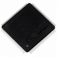
ST92F150CV1TB STMicroelectronics, ST92F150CV1TB Datasheet - Page 61

ST92F150CV1TB
Manufacturer Part Number
ST92F150CV1TB
Description
MCU 8BIT 128K FLASH 100TQFP
Manufacturer
STMicroelectronics
Series
ST9r
Datasheet
1.ST92F150CV1TB.pdf
(429 pages)
Specifications of ST92F150CV1TB
Core Processor
ST9
Core Size
8/16-Bit
Speed
24MHz
Connectivity
CAN, EBI/EMI, I²C, LIN, SCI, SPI
Peripherals
DMA, LVD, POR, PWM, WDT
Number Of I /o
77
Program Memory Size
128KB (128K x 8)
Program Memory Type
FLASH
Eeprom Size
1K x 8
Ram Size
4K x 8
Voltage - Supply (vcc/vdd)
4.5 V ~ 5.5 V
Data Converters
A/D 16x10b
Oscillator Type
Internal
Operating Temperature
-40°C ~ 105°C
Package / Case
100-TQFP, 100-VQFP
Processor Series
ST92F15x
Core
ST9
Data Bus Width
8 bit, 16 bit
Data Ram Size
6 KB
Interface Type
CAN, I2C, SCI, SPI
Maximum Clock Frequency
24 MHz
Number Of Programmable I/os
80
Number Of Timers
5 x 16 bit
Operating Supply Voltage
4.5 V to 5.5 V
Maximum Operating Temperature
+ 105 C
Mounting Style
SMD/SMT
Development Tools By Supplier
ST92F150-EPB
Minimum Operating Temperature
- 40 C
On-chip Adc
16 bit x 10 bit
Lead Free Status / RoHS Status
Lead free / RoHS Compliant
Other names
497-4883
Available stocks
Company
Part Number
Manufacturer
Quantity
Price
Company:
Part Number:
ST92F150CV1TB
Manufacturer:
STMicroelectronics
Quantity:
10 000
- Current page: 61 of 429
- Download datasheet (8Mb)
3.5 PROTECTION STRATEGY
The protection bits are stored in the 4 locations
from 231FFCh to 231FFFh (see
All the available protections are forced active dur-
ing reset, then in the initialisation phase they are
read from the TestFlash.
The protections are stored in 2 Non Volatile Regis-
ters. Other 2 Non Volatile Registers can be used
as a password to re-enable test modes once they
have been disabled.
The protections can be programmed using the Set
Protection operation (see Control Registers para-
graph), that can be executed from all the internal
or external memories except the Flash or Test-
Flash itself.
The TestFlash area (230000h to 231F7Fh) is al-
ways protected against write access.
Figure 34. Protection Register Map
3.5.1 Non Volatile Registers
The 4 Non Volatile Registers used to store the pro-
tection bits for the different protection features are
one time programmable by the user.
Access to these registers is controlled by the pro-
tections related to the TestFlash. Since the code to
program the Protection Registers cannot be
fetched by the Flash or the TestFlash memories,
this means that, once the APRO or APBR bits in
the NVAPR register are programmed, it is no long-
er possible to modify any of the protection bits. For
this reason the NV Password, if needed, must be
set with the same Set Protection operation used to
program these bits. For the same reason it is
strongly advised to never program the WPBR bit in
the NVWPR register, as this will prevent any fur-
ther write access to the TestFlash, and conse-
quently to the Protection Registers.
ST92F124/F150/F250 - SINGLE VOLTAGE FLASH & E3 TM (EMULATED EEPROM)
231FFCh
231FFDh
231FFEh
231FFFh
NVPWD0
NVWPR
NVPWD1
NVAPR
Figure
34).
NON VOLATILE ACCESS PROTECTION REG-
ISTER (NVAPR)
Address: 231FFCh - Read/Write
Delivery value: 1111 1111 (FFh)
Bit 7 = Reserved.
Bit 6 = APRO: FLASH access protection.
This bit, if programmed at 0, disables any access
(read/write) to operands mapped inside the Flash
address space (
instruction is fetched from the TestFlash or from
the Flash itself.
0: ROM protection on
1: ROM protection off
Bit 5 = APBR: TestFlash access protection.
This bit, if programmed at 0, disables any access
(read/write) to operands mapped inside the Test-
Flash, the OTP and the protection registers, un-
less the current instruction is fetched from the
TestFlash or the OTP area.
0: TestFlash protection on
1: TestFlash protection off
Bit 4 = APEE:
This bit, if programmed at 0, disables any access
(read/write) to operands mapped inside the
address space, unless the current instruction is
fetched from the TestFlash or from the Flash, or
from the
0:
1:
Bit 3 = APEX: Access Protection from External
memory.
This bit, if programmed at 0, disables any access
(read/write) to operands mapped inside the ad-
dress space of one of the internal memories (Test-
Flash, Flash,
is fetched from an external memory.
0: Protection from external memory on
1: Protection from external memory off
E
E
7
1
3 TM
3 TM
APRO APBR APEE APEX PWT2 PWT1 PWT0
protection on
protection off
6
E
3 TM
E
E
itself.
3 TM
5
E
3 TM
3 TM
, RAM), if the current instruction
access protection.
4
excluded), unless the current
3
2
1
61/429
E
0
3 TM
9
Related parts for ST92F150CV1TB
Image
Part Number
Description
Manufacturer
Datasheet
Request
R

Part Number:
Description:
BOARD PROGRAM FOR ST92F150 MCU
Manufacturer:
STMicroelectronics
Datasheet:

Part Number:
Description:
BOARD EVALUATION FOR ST9 SERIES
Manufacturer:
STMicroelectronics
Datasheet:

Part Number:
Description:
BOARD EMULATOR FOR ST9 SERIES
Manufacturer:
STMicroelectronics
Datasheet:

Part Number:
Description:
MCU, MPU & DSP Development Tools ST9 Dedication Board
Manufacturer:
STMicroelectronics
Datasheet:

Part Number:
Description:
STMicroelectronics [RIPPLE-CARRY BINARY COUNTER/DIVIDERS]
Manufacturer:
STMicroelectronics
Datasheet:

Part Number:
Description:
STMicroelectronics [LIQUID-CRYSTAL DISPLAY DRIVERS]
Manufacturer:
STMicroelectronics
Datasheet:

Part Number:
Description:
BOARD EVAL FOR MEMS SENSORS
Manufacturer:
STMicroelectronics
Datasheet:

Part Number:
Description:
NPN TRANSISTOR POWER MODULE
Manufacturer:
STMicroelectronics
Datasheet:

Part Number:
Description:
TURBOSWITCH ULTRA-FAST HIGH VOLTAGE DIODE
Manufacturer:
STMicroelectronics
Datasheet:

Part Number:
Description:
Manufacturer:
STMicroelectronics
Datasheet:

Part Number:
Description:
DIODE / SCR MODULE
Manufacturer:
STMicroelectronics
Datasheet:

Part Number:
Description:
DIODE / SCR MODULE
Manufacturer:
STMicroelectronics
Datasheet:


