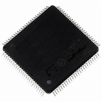
ST92F150CV1TB STMicroelectronics, ST92F150CV1TB Datasheet - Page 177

ST92F150CV1TB
Manufacturer Part Number
ST92F150CV1TB
Description
MCU 8BIT 128K FLASH 100TQFP
Manufacturer
STMicroelectronics
Series
ST9r
Datasheet
1.ST92F150CV1TB.pdf
(429 pages)
Specifications of ST92F150CV1TB
Core Processor
ST9
Core Size
8/16-Bit
Speed
24MHz
Connectivity
CAN, EBI/EMI, I²C, LIN, SCI, SPI
Peripherals
DMA, LVD, POR, PWM, WDT
Number Of I /o
77
Program Memory Size
128KB (128K x 8)
Program Memory Type
FLASH
Eeprom Size
1K x 8
Ram Size
4K x 8
Voltage - Supply (vcc/vdd)
4.5 V ~ 5.5 V
Data Converters
A/D 16x10b
Oscillator Type
Internal
Operating Temperature
-40°C ~ 105°C
Package / Case
100-TQFP, 100-VQFP
Processor Series
ST92F15x
Core
ST9
Data Bus Width
8 bit, 16 bit
Data Ram Size
6 KB
Interface Type
CAN, I2C, SCI, SPI
Maximum Clock Frequency
24 MHz
Number Of Programmable I/os
80
Number Of Timers
5 x 16 bit
Operating Supply Voltage
4.5 V to 5.5 V
Maximum Operating Temperature
+ 105 C
Mounting Style
SMD/SMT
Development Tools By Supplier
ST92F150-EPB
Minimum Operating Temperature
- 40 C
On-chip Adc
16 bit x 10 bit
Lead Free Status / RoHS Status
Lead free / RoHS Compliant
Other names
497-4883
Available stocks
Company
Part Number
Manufacturer
Quantity
Price
Company:
Part Number:
ST92F150CV1TB
Manufacturer:
STMicroelectronics
Quantity:
10 000
- Current page: 177 of 429
- Download datasheet (8Mb)
EXTENDED FUNCTION TIMER (Cont’d)
10.3.3.7 Pulse Width Modulation Mode
Pulse Width Modulation mode enables the gener-
ation of a signal with a frequency and pulse length
determined by the value of the OC1R and OC2R
registers.
The pulse width modulation mode uses the com-
plete Output Compare 1 function plus the OC2R
register.
Procedure
To use pulse width modulation mode select the fol-
lowing in the CR1 register:
– Using the OLVL1 bit, select the level to be ap-
– Using the OLVL2 bit, select the level to be ap-
And select the following in the CR2 register:
– Set OC1E bit: the OCMP1 pin is then dedicated
– Set the PWM bit.
– Select the timer clock CC[1:0] bits (see
Load the OC2R register with the value corre-
sponding to the period of the signal.
Load the OC1R register with the value corre-
sponding to the length of the pulse if (OLVL1=0
and OLVL2=1).
If OLVL1=1 and OLVL2=0 the length of the pulse
is the difference between the OC2R and OC1R
registers.
The OC
ing application can be calculated using the follow-
ing formula:
Where:
The Output Compare 2 event causes the counter
to be initialized to FFFCh (See
plied to the OCMP1 pin after a successful com-
parison with OC1R register.
plied to the OCMP1 pin after a successful com-
parison with OC2R register.
to the output compare 1 function.
36).
– t = Desired output compare period (seconds)
–
– CC1-CC0 = Timer clock prescaler
INTCLK
i
R register value required for a specific tim-
OCiR Value =
= Internal clock frequency
CC[1:0]
t
* INTCLK
Figure
- 5
100).
Table
Notes:
– After a write instruction to the OCiHR register,
– The OCF1 bit cannot be set by hardware in PWM
– The Input Capture function is available in PWM
– When Counter = OC2R, then the OCF2 bit will be
– When the Pulse Width Modulation (PWM) and
– The value loaded in register OC2R must always
– When OC1R >OC2R, no waveform will be gen-
– When OC2R = OC1R, a square waveform will
– When OC2R is loaded with FFFC (the counter
– When OC1R is loaded with FFFC (the counter
– When FOLV1 bit is set and PWM bit is set, then
the output compare function is inhibited until the
OCiLR register is also written.
mode, but the OCF2 bit is set every time the
counter matches the OC2R register.
mode.
set. This can generate an interrupt if OCIE is set
or OCIE is reset and OC2IE is set. This interrupt
is useful in applications where the pulse-width or
period needs to be changed interactively.
One Pulse Mode (OPM) bits are both set, the
PWM mode is the only active mode.
be greater than the value in register OC1R in or-
der to produce meaningful waveforms. Note that
0000h is considerred to be greater than FFFCh
or FFFDh or FFFEh or FFFFh.
erated.
be generated as in
reset value) then no waveform will be generated
& the counter will remain stuck at FFFC.
reset value) then the waveform will be generated
as in
PWM mode is the active one. But if FOLV2 bit is
set then the OLVL2 bit will appear on OCMP2
(when OC2E bit = 1).
EXTENDED FUNCTION TIMER (EFT)
Figure 100
Counter
= OC1R
Counter
= OC2R
When
When
Pulse Width Modulation cycle
Figure 100
OCMP1 = OLVL2
OCMP1 = OLVL1
Counter is reset
to FFFCh
177/429
9
Related parts for ST92F150CV1TB
Image
Part Number
Description
Manufacturer
Datasheet
Request
R

Part Number:
Description:
BOARD PROGRAM FOR ST92F150 MCU
Manufacturer:
STMicroelectronics
Datasheet:

Part Number:
Description:
BOARD EVALUATION FOR ST9 SERIES
Manufacturer:
STMicroelectronics
Datasheet:

Part Number:
Description:
BOARD EMULATOR FOR ST9 SERIES
Manufacturer:
STMicroelectronics
Datasheet:

Part Number:
Description:
MCU, MPU & DSP Development Tools ST9 Dedication Board
Manufacturer:
STMicroelectronics
Datasheet:

Part Number:
Description:
STMicroelectronics [RIPPLE-CARRY BINARY COUNTER/DIVIDERS]
Manufacturer:
STMicroelectronics
Datasheet:

Part Number:
Description:
STMicroelectronics [LIQUID-CRYSTAL DISPLAY DRIVERS]
Manufacturer:
STMicroelectronics
Datasheet:

Part Number:
Description:
BOARD EVAL FOR MEMS SENSORS
Manufacturer:
STMicroelectronics
Datasheet:

Part Number:
Description:
NPN TRANSISTOR POWER MODULE
Manufacturer:
STMicroelectronics
Datasheet:

Part Number:
Description:
TURBOSWITCH ULTRA-FAST HIGH VOLTAGE DIODE
Manufacturer:
STMicroelectronics
Datasheet:

Part Number:
Description:
Manufacturer:
STMicroelectronics
Datasheet:

Part Number:
Description:
DIODE / SCR MODULE
Manufacturer:
STMicroelectronics
Datasheet:

Part Number:
Description:
DIODE / SCR MODULE
Manufacturer:
STMicroelectronics
Datasheet:


