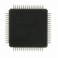
HD64F3664FPV Renesas Electronics America, HD64F3664FPV Datasheet - Page 122

HD64F3664FPV
Manufacturer Part Number
HD64F3664FPV
Description
IC H8/3664 MCU FLASH 32K 64LQFP
Manufacturer
Renesas Electronics America
Series
H8® H8/300H Tinyr
Specifications of HD64F3664FPV
Core Size
16-Bit
Program Memory Size
32KB (32K x 8)
Oscillator Type
External
Core Processor
H8/300H
Speed
16MHz
Connectivity
I²C, SCI
Peripherals
PWM, WDT
Number Of I /o
29
Program Memory Type
FLASH
Ram Size
2K x 8
Voltage - Supply (vcc/vdd)
3 V ~ 5.5 V
Data Converters
A/D 8x10b
Operating Temperature
-20°C ~ 75°C
Package / Case
64-LQFP
No. Of I/o's
29
Ram Memory Size
2KB
Cpu Speed
16MHz
No. Of Timers
4
Digital Ic Case Style
LQFP
Supply Voltage
RoHS Compliant
Controller Family/series
H8/300H
Rohs Compliant
Yes
Lead Free Status / RoHS Status
Lead free / RoHS Compliant
Eeprom Size
-
Lead Free Status / RoHS Status
Lead free / RoHS Compliant
Available stocks
Company
Part Number
Manufacturer
Quantity
Price
Company:
Part Number:
HD64F3664FPV
Manufacturer:
MURATA
Quantity:
34 000
Company:
Part Number:
HD64F3664FPV
Manufacturer:
HD
Quantity:
465
Company:
Part Number:
HD64F3664FPV
Manufacturer:
Renesas Electronics America
Quantity:
10 000
Part Number:
HD64F3664FPV
Manufacturer:
RENESAS/瑞萨
Quantity:
20 000
- Current page: 122 of 420
- Download datasheet (3Mb)
When changing to boot mode, the boot program built into this LSI is initiated. The boot program
transfers the programming control program from the externally-connected host to on-chip RAM
via SCI3. After erasing the entire flash memory, the programming control program is executed.
This can be used for programming initial values in the on-board state or for a forcible return when
programming/erasing can no longer be done in user program mode. In user program mode,
individual blocks can be erased and programmed by branching to the user program/erase control
program prepared by the user.
Table 7.1
TEST
0
0
1
Legend: X: Don’t care.
7.3.1
Table 7.2 shows the boot mode operations between reset end and branching to the programming
control program.
1. When boot mode is used, the flash memory programming control program must be prepared in
2. SCI3 should be set to asynchronous mode, and the transfer format as follows: 8-bit data, 1 stop
3. When the boot program is initiated, the chip measures the low-level period of asynchronous
4. After matching the bit rates, the chip transmits one H'00 byte to the host to indicate the
5. In boot mode, a part of the on-chip RAM area is used by the boot program. The area H'F780 to
Rev. 5.00, 03/04, page 94 of 388
the host beforehand. Prepare a programming control program in accordance with the
description in section 7.4, Flash Memory Programming/Erasing.
bit, and no parity.
SCI communication data (H'00) transmitted continuously from the host. The chip then
calculates the bit rate of transmission from the host, and adjusts the SCI3 bit rate to match that
of the host. The reset should end with the RxD pin high. The RxD and TxD pins should be
pulled up on the board if necessary. After the reset is complete, it takes approximately 100
states before the chip is ready to measure the low-level period.
completion of bit rate adjustment. The host should confirm that this adjustment end indication
(H'00) has been received normally, and transmit one H'55 byte to the chip. If reception could
not be performed normally, initiate boot mode again by a reset. Depending on the host's
transfer bit rate and system clock frequency of this LSI, there will be a discrepancy between
the bit rates of the host and the chip. To operate the SCI properly, set the host's transfer bit
rate and system clock frequency of this LSI within the ranges listed in table 7.3.
H'FEEF is the area to which the programming control program is transferred from the host.
Boot Mode
NMI
1
0
X
Setting Programming Modes
P85
X
1
X
PB0
X
X
0
PB1
X
X
0
PB2
X
X
0
LSI State after Reset End
User Mode
Boot Mode
Programmer Mode
Related parts for HD64F3664FPV
Image
Part Number
Description
Manufacturer
Datasheet
Request
R

Part Number:
Description:
KIT STARTER FOR M16C/29
Manufacturer:
Renesas Electronics America
Datasheet:

Part Number:
Description:
KIT STARTER FOR R8C/2D
Manufacturer:
Renesas Electronics America
Datasheet:

Part Number:
Description:
R0K33062P STARTER KIT
Manufacturer:
Renesas Electronics America
Datasheet:

Part Number:
Description:
KIT STARTER FOR R8C/23 E8A
Manufacturer:
Renesas Electronics America
Datasheet:

Part Number:
Description:
KIT STARTER FOR R8C/25
Manufacturer:
Renesas Electronics America
Datasheet:

Part Number:
Description:
KIT STARTER H8S2456 SHARPE DSPLY
Manufacturer:
Renesas Electronics America
Datasheet:

Part Number:
Description:
KIT STARTER FOR R8C38C
Manufacturer:
Renesas Electronics America
Datasheet:

Part Number:
Description:
KIT STARTER FOR R8C35C
Manufacturer:
Renesas Electronics America
Datasheet:

Part Number:
Description:
KIT STARTER FOR R8CL3AC+LCD APPS
Manufacturer:
Renesas Electronics America
Datasheet:

Part Number:
Description:
KIT STARTER FOR RX610
Manufacturer:
Renesas Electronics America
Datasheet:

Part Number:
Description:
KIT STARTER FOR R32C/118
Manufacturer:
Renesas Electronics America
Datasheet:

Part Number:
Description:
KIT DEV RSK-R8C/26-29
Manufacturer:
Renesas Electronics America
Datasheet:

Part Number:
Description:
KIT STARTER FOR SH7124
Manufacturer:
Renesas Electronics America
Datasheet:

Part Number:
Description:
KIT STARTER FOR H8SX/1622
Manufacturer:
Renesas Electronics America
Datasheet:


