HD64F3664FPV Renesas Electronics America, HD64F3664FPV Datasheet - Page 9
HD64F3664FPV
Manufacturer Part Number
HD64F3664FPV
Description
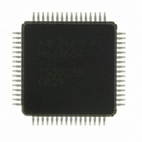
IC H8/3664 MCU FLASH 32K 64LQFP
Manufacturer
Renesas Electronics America
Series
H8® H8/300H Tinyr
Specifications of HD64F3664FPV
Core Size
16-Bit
Program Memory Size
32KB (32K x 8)
Oscillator Type
External
Core Processor
H8/300H
Speed
16MHz
Connectivity
I²C, SCI
Peripherals
PWM, WDT
Number Of I /o
29
Program Memory Type
FLASH
Ram Size
2K x 8
Voltage - Supply (vcc/vdd)
3 V ~ 5.5 V
Data Converters
A/D 8x10b
Operating Temperature
-20°C ~ 75°C
Package / Case
64-LQFP
No. Of I/o's
29
Ram Memory Size
2KB
Cpu Speed
16MHz
No. Of Timers
4
Digital Ic Case Style
LQFP
Supply Voltage
RoHS Compliant
Controller Family/series
H8/300H
Rohs Compliant
Yes
Lead Free Status / RoHS Status
Lead free / RoHS Compliant
Eeprom Size
-
Lead Free Status / RoHS Status
Lead free / RoHS Compliant
Available stocks
Company
Part Number
Manufacturer
Quantity
Price
Company:

Part Number:
HD64F3664FPV
Manufacturer:
MURATA
Quantity:
34 000
Company:
Part Number:
HD64F3664FPV
Manufacturer:
HD
Quantity:
465
Company:
Part Number:
HD64F3664FPV
Manufacturer:
Renesas Electronics America
Quantity:
10 000
Part Number:
HD64F3664FPV
Manufacturer:
RENESAS/瑞萨
Quantity:
20 000


Section 1 Overview............................................................................................1
1.1
1.2
1.3
1.4
Section 2 CPU....................................................................................................11
2.1
2.2
2.3
2.4
2.5
2.6
2.7
2.8
Section 3 Exception Handling ...........................................................................47
3.1
3.2
3.3
Features............................................................................................................................. 1
Internal Block Diagram..................................................................................................... 2
Pin Arrangement ............................................................................................................... 4
Pin Functions .................................................................................................................... 8
Address Space and Memory Map ..................................................................................... 12
Register Configuration...................................................................................................... 15
2.2.1
2.2.2
2.2.3
Data Formats..................................................................................................................... 19
2.3.1
2.3.2
Instruction Set ................................................................................................................... 22
2.4.1
2.4.2
Addressing Modes and Effective Address Calculation..................................................... 33
2.5.1
2.5.2
Basic Bus Cycle ................................................................................................................ 38
2.6.1
2.6.2
CPU States ........................................................................................................................ 40
Usage Notes ...................................................................................................................... 41
2.8.1
2.8.2
2.8.3
Exception Sources and Vector Address ............................................................................ 47
Register Descriptions ........................................................................................................ 49
3.2.1
3.2.2
3.2.3
3.2.4
3.2.5
Reset Exception Handling................................................................................................. 54
General Registers................................................................................................. 16
Program Counter (PC) ......................................................................................... 17
Condition-Code Register (CCR).......................................................................... 17
General Register Data Formats ............................................................................ 19
Memory Data Formats ......................................................................................... 21
Table of Instructions Classified by Function ....................................................... 22
Basic Instruction Formats .................................................................................... 31
Addressing Modes ............................................................................................... 33
Effective Address Calculation ............................................................................. 36
Access to On-Chip Memory (RAM, ROM)......................................................... 38
On-Chip Peripheral Modules ............................................................................... 39
Notes on Data Access to Empty Areas ................................................................ 41
EEPMOV Instruction........................................................................................... 41
Bit Manipulation Instruction................................................................................ 41
Interrupt Edge Select Register 1 (IEGR1) ........................................................... 49
Interrupt Edge Select Register 2 (IEGR2) ........................................................... 50
Interrupt Enable Register 1 (IENR1) ................................................................... 51
Interrupt Flag Register 1 (IRR1).......................................................................... 52
Wakeup Interrupt Flag Register (IWPR) ............................................................. 53
Contents
Rev. 5.00, 03/04, page ix of xxviii
Related parts for HD64F3664FPV
Image
Part Number
Description
Manufacturer
Datasheet
Request
R


Part Number:
Description:
KIT STARTER FOR M16C/29
Manufacturer:
Renesas Electronics America
Datasheet:

Part Number:
Description:
KIT STARTER FOR R8C/2D
Manufacturer:
Renesas Electronics America
Datasheet:

Part Number:
Description:
R0K33062P STARTER KIT
Manufacturer:
Renesas Electronics America
Datasheet:

Part Number:
Description:
KIT STARTER FOR R8C/23 E8A
Manufacturer:
Renesas Electronics America
Datasheet:

Part Number:
Description:
KIT STARTER FOR R8C/25
Manufacturer:
Renesas Electronics America
Datasheet:

Part Number:
Description:
KIT STARTER H8S2456 SHARPE DSPLY
Manufacturer:
Renesas Electronics America
Datasheet:

Part Number:
Description:
KIT STARTER FOR R8C38C
Manufacturer:
Renesas Electronics America
Datasheet:

Part Number:
Description:
KIT STARTER FOR R8C35C
Manufacturer:
Renesas Electronics America
Datasheet:

Part Number:
Description:
KIT STARTER FOR R8CL3AC+LCD APPS
Manufacturer:
Renesas Electronics America
Datasheet:
Part Number:
Description:
KIT STARTER FOR RX610
Manufacturer:
Renesas Electronics America
Datasheet:

Part Number:
Description:
KIT STARTER FOR R32C/118
Manufacturer:
Renesas Electronics America
Datasheet:

Part Number:
Description:
KIT DEV RSK-R8C/26-29
Manufacturer:
Renesas Electronics America
Datasheet:

Part Number:
Description:
KIT STARTER FOR SH7124
Manufacturer:
Renesas Electronics America
Datasheet:

Part Number:
Description:
KIT STARTER FOR H8SX/1622
Manufacturer:
Renesas Electronics America
Datasheet: