ATTINY48-MMU Atmel, ATTINY48-MMU Datasheet - Page 115
ATTINY48-MMU
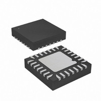
Manufacturer Part Number
ATTINY48-MMU
Description
MCU AVR 5K FLASH 12MHZ 28-QFN
Manufacturer
Atmel
Series
AVR® ATtinyr
Specifications of ATTINY48-MMU
Core Processor
AVR
Core Size
8-Bit
Speed
12MHz
Connectivity
I²C, SPI
Peripherals
Brown-out Detect/Reset, POR, WDT
Number Of I /o
24
Program Memory Size
4KB (2K x 16)
Program Memory Type
FLASH
Eeprom Size
64 x 8
Ram Size
256 x 8
Voltage - Supply (vcc/vdd)
1.8 V ~ 5.5 V
Data Converters
A/D 6x10b
Oscillator Type
Internal
Operating Temperature
-40°C ~ 85°C
Package / Case
28-VQFN Exposed Pad, 28-HVQFN, 28-SQFN, 28-DHVQFN
Processor Series
ATTINY4x
Core
AVR8
Data Bus Width
8 bit
Data Ram Size
256 B
Interface Type
2-Wire, I2S, SPI
Maximum Clock Frequency
12 MHz
Number Of Programmable I/os
24
Number Of Timers
2
Maximum Operating Temperature
+ 85 C
Mounting Style
SMD/SMT
3rd Party Development Tools
EWAVR, EWAVR-BL
Development Tools By Supplier
ATAVRDRAGON, ATSTK500, ATSTK600, ATAVRISP2, ATAVRONEKIT
Minimum Operating Temperature
- 40 C
On-chip Adc
10 bit, 6 Channel
Package
28VQFN EP
Device Core
AVR
Family Name
ATtiny
Maximum Speed
12 MHz
Operating Supply Voltage
2.5|3.3|5 V
For Use With
ATAVRDRAGON - KIT DRAGON 32KB FLASH MEM AVR
Lead Free Status / RoHS Status
Lead free / RoHS Compliant


12.11.9
8008G–AVR–04/11
TIFR1 – Timer/Counter1 Interrupt Flag Register
• Bit 5 – ICIE1: Timer/Counter1, Input Capture Interrupt Enable
When this bit is written to one, and the I-flag in the Status Register is set (interrupts globally
enabled), the Timer/Counter1 Input Capture interrupt is enabled. The corresponding Interrupt
Vector (see “Interrupts” on page 52) is executed when the ICF1 Flag, located in TIFR1, is set.
• Bits 4:3 – Res: Reserved Bits
These bits are reserved and will always read zero.
• Bit 2 – OCIE1B: Timer/Counter1, Output Compare B Match Interrupt Enable
When this bit is written to one, and the I-flag in the Status Register is set (interrupts globally
enabled), the Timer/Counter1 Output Compare B Match interrupt is enabled. The corresponding
Interrupt Vector (see “Interrupts” on page 52) is executed when the OCF1B Flag, located in
TIFR1, is set.
• Bit 1 – OCIE1A: Timer/Counter1, Output Compare A Match Interrupt Enable
When this bit is written to one, and the I-flag in the Status Register is set (interrupts globally
enabled), the Timer/Counter1 Output Compare A Match interrupt is enabled. The corresponding
Interrupt Vector (see “Interrupts” on page 52) is executed when the OCF1A Flag, located in
TIFR1, is set.
• Bit 0 – TOIE1: Timer/Counter1, Overflow Interrupt Enable
When this bit is written to one, and the I-flag in the Status Register is set (interrupts globally
enabled), the Timer/Counter1 Overflow interrupt is enabled. The corresponding Interrupt Vector
(See “Watchdog Timer” on page
• Bits 7:6 – Res: Reserved Bits
These bits are reserved and will always read zero.
• Bit 5 – ICF1: Timer/Counter1, Input Capture Flag
This flag is set when a capture event occurs on the ICP1 pin. When the Input Capture Register
(ICR1) is set by the WGM1[3:0] to be used as the TOP value, the ICF1 Flag is set when the
counter reaches the TOP value.
ICF1 is automatically cleared when the Input Capture Interrupt Vector is executed. Alternatively,
ICF1 can be cleared by writing a logic one to its bit location.
• Bits 4:3 – Res: Reserved Bits
These bits are reserved and will always read zero.
• Bit 2 – OCF1B: Timer/Counter1, Output Compare B Match Flag
This flag is set in the timer clock cycle after the counter (TCNT1) value matches the Output
Compare Register B (OCR1B).
Note that a Forced Output Compare (FOC1B) strobe will not set the OCF1B Flag.
Bit
0x16 (0x36)
Read/Write
Initial Value
R
7
–
0
R
6
–
0
46.) is executed when the TOV1 Flag, located in TIFR1, is set.
ICF1
R/W
5
0
R
4
–
0
R
3
–
0
OCF1B
R/W
2
0
OCF1A
R/W
1
0
ATtiny48/88
TOV1
R/W
0
0
TIFR1
115
Related parts for ATTINY48-MMU
Image
Part Number
Description
Manufacturer
Datasheet
Request
R

Part Number:
Description:
Manufacturer:
Atmel Corporation
Datasheet:

Part Number:
Description:
MCU AVR 4K ISP FLASH 1.8V 32TQFP
Manufacturer:
Atmel
Datasheet:

Part Number:
Description:
MCU AVR 4K ISP FLASH 1.8V 32-QFN
Manufacturer:
Atmel
Datasheet:

Part Number:
Description:
MCU AVR 4K ISP FLASH 1.8V 28-DIP
Manufacturer:
Atmel
Datasheet:

Part Number:
Description:
MCU AVR 4KB FLASH 12MHZ 32TQFP
Manufacturer:
Atmel
Datasheet:
Part Number:
Description:
MCU AVR 4KB FLASH 12MHZ 32QFN
Manufacturer:
Atmel
Datasheet:

Part Number:
Description:
MCU AVR 4KB FLASH 12MHZ 28-VQFN
Manufacturer:
Atmel
Datasheet:
Part Number:
Description:
MCU AVR 4KB FLASH 12MHZ 28QFN
Manufacturer:
Atmel
Datasheet:
Part Number:
Description:
8-bit Microcontrollers - MCU 4KB FL,64B EE, 256B SRAM-12MHz
Manufacturer:
Atmel
Part Number:
Description:
8-bit Microcontrollers - MCU Microcontroller
Manufacturer:
Atmel
Part Number:
Description:
Manufacturer:
Atmel Corporation
Datasheet: