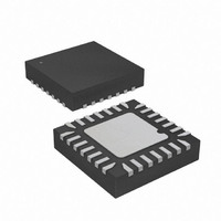
ATTINY48-MMU Atmel, ATTINY48-MMU Datasheet - Page 182

ATTINY48-MMU
Manufacturer Part Number
ATTINY48-MMU
Description
MCU AVR 5K FLASH 12MHZ 28-QFN
Manufacturer
Atmel
Series
AVR® ATtinyr
Specifications of ATTINY48-MMU
Core Processor
AVR
Core Size
8-Bit
Speed
12MHz
Connectivity
I²C, SPI
Peripherals
Brown-out Detect/Reset, POR, WDT
Number Of I /o
24
Program Memory Size
4KB (2K x 16)
Program Memory Type
FLASH
Eeprom Size
64 x 8
Ram Size
256 x 8
Voltage - Supply (vcc/vdd)
1.8 V ~ 5.5 V
Data Converters
A/D 6x10b
Oscillator Type
Internal
Operating Temperature
-40°C ~ 85°C
Package / Case
28-VQFN Exposed Pad, 28-HVQFN, 28-SQFN, 28-DHVQFN
Processor Series
ATTINY4x
Core
AVR8
Data Bus Width
8 bit
Data Ram Size
256 B
Interface Type
2-Wire, I2S, SPI
Maximum Clock Frequency
12 MHz
Number Of Programmable I/os
24
Number Of Timers
2
Maximum Operating Temperature
+ 85 C
Mounting Style
SMD/SMT
3rd Party Development Tools
EWAVR, EWAVR-BL
Development Tools By Supplier
ATAVRDRAGON, ATSTK500, ATSTK600, ATAVRISP2, ATAVRONEKIT
Minimum Operating Temperature
- 40 C
On-chip Adc
10 bit, 6 Channel
Package
28VQFN EP
Device Core
AVR
Family Name
ATtiny
Maximum Speed
12 MHz
Operating Supply Voltage
2.5|3.3|5 V
For Use With
ATAVRDRAGON - KIT DRAGON 32KB FLASH MEM AVR
Lead Free Status / RoHS Status
Lead free / RoHS Compliant
- Current page: 182 of 302
- Download datasheet (9Mb)
18.4
18.5
18.6
18.6.1
182
Software Break Points
Limitations of debugWIRE
Register Description
ATtiny48/88
DWDR – debugWire Data Register
When designing a system where debugWIRE will be used, the following observations must be
made for correct operation:
debugWIRE supports Program memory Break Points by the AVR Break instruction. Setting a
Break Point in AVR Studio
tion replaced by the BREAK instruction will be stored. When program execution is continued, the
stored instruction will be executed before continuing from the Program memory. A break can be
inserted manually by putting the BREAK instruction in the program.
The Flash must be re-programmed each time a Break Point is changed. This is automatically
handled by AVR Studio through the debugWIRE interface. The use of Break Points will therefore
reduce the Flash Data retention. Devices used for debugging purposes should not be shipped to
end customers.
The debugWIRE communication pin (dW) is physically located on the same pin as External
Reset (RESET). An External Reset source is therefore not supported when the debugWIRE is
enabled.
The debugWIRE system accurately emulates all I/O functions when running at full speed, i.e.,
when the program in the CPU is running. When the CPU is stopped, care must be taken while
accessing some of the I/O Registers via the debugger (AVR Studio).
The debugWIRE interface is asynchronous, which means that the debugger needs to synchro-
nize to the system clock. If the system clock is changed by software (e.g. by writing CLKPS bits)
communication via debugWIRE may fail. Also, clock frequencies below 100 kHz may cause
communication problems.
A programmed DWEN Fuse enables some parts of the clock system to be running in all sleep
modes. This will increase the power consumption while in sleep. Thus, the DWEN Fuse should
be disabled when debugWire is not used.
The DWDR Register provides a communication channel from the running program in the MCU
to the debugger. This register is only accessible by the debugWIRE and can therefore not be
used as a general purpose register in the normal operations.
Bit
0x31 (0x51)
Read/Write
Initial Value
• Pull-up resistors on the dW/(RESET) line must not be smaller than 10kΩ. The pull-up resistor
• Connecting the RESET pin directly to V
• Capacitors connected to the RESET pin must be disconnected when using debugWire.
• All external reset sources must be disconnected.
is not required for debugWIRE functionality.
R/W
7
0
R/W
®
6
0
will insert a BREAK instruction in the Program memory. The instruc-
R/W
5
0
CC
R/W
4
0
DWDR[7:0]
will not work.
R/W
3
0
R/W
2
0
R/W
1
0
R/W
0
0
8008G–AVR–04/11
DWDR
Related parts for ATTINY48-MMU
Image
Part Number
Description
Manufacturer
Datasheet
Request
R

Part Number:
Description:
Manufacturer:
Atmel Corporation
Datasheet:

Part Number:
Description:
MCU AVR 4K ISP FLASH 1.8V 32TQFP
Manufacturer:
Atmel
Datasheet:

Part Number:
Description:
MCU AVR 4K ISP FLASH 1.8V 32-QFN
Manufacturer:
Atmel
Datasheet:

Part Number:
Description:
MCU AVR 4K ISP FLASH 1.8V 28-DIP
Manufacturer:
Atmel
Datasheet:

Part Number:
Description:
MCU AVR 4KB FLASH 12MHZ 32TQFP
Manufacturer:
Atmel
Datasheet:

Part Number:
Description:
MCU AVR 4KB FLASH 12MHZ 32QFN
Manufacturer:
Atmel
Datasheet:

Part Number:
Description:
MCU AVR 4KB FLASH 12MHZ 28-VQFN
Manufacturer:
Atmel
Datasheet:

Part Number:
Description:
MCU AVR 4KB FLASH 12MHZ 28QFN
Manufacturer:
Atmel
Datasheet:

Part Number:
Description:
8-bit Microcontrollers - MCU 4KB FL,64B EE, 256B SRAM-12MHz
Manufacturer:
Atmel

Part Number:
Description:
8-bit Microcontrollers - MCU Microcontroller
Manufacturer:
Atmel

Part Number:
Description:
Manufacturer:
Atmel Corporation
Datasheet:


