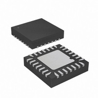
ATTINY48-MMU Atmel, ATTINY48-MMU Datasheet - Page 36

ATTINY48-MMU
Manufacturer Part Number
ATTINY48-MMU
Description
MCU AVR 5K FLASH 12MHZ 28-QFN
Manufacturer
Atmel
Series
AVR® ATtinyr
Specifications of ATTINY48-MMU
Core Processor
AVR
Core Size
8-Bit
Speed
12MHz
Connectivity
I²C, SPI
Peripherals
Brown-out Detect/Reset, POR, WDT
Number Of I /o
24
Program Memory Size
4KB (2K x 16)
Program Memory Type
FLASH
Eeprom Size
64 x 8
Ram Size
256 x 8
Voltage - Supply (vcc/vdd)
1.8 V ~ 5.5 V
Data Converters
A/D 6x10b
Oscillator Type
Internal
Operating Temperature
-40°C ~ 85°C
Package / Case
28-VQFN Exposed Pad, 28-HVQFN, 28-SQFN, 28-DHVQFN
Processor Series
ATTINY4x
Core
AVR8
Data Bus Width
8 bit
Data Ram Size
256 B
Interface Type
2-Wire, I2S, SPI
Maximum Clock Frequency
12 MHz
Number Of Programmable I/os
24
Number Of Timers
2
Maximum Operating Temperature
+ 85 C
Mounting Style
SMD/SMT
3rd Party Development Tools
EWAVR, EWAVR-BL
Development Tools By Supplier
ATAVRDRAGON, ATSTK500, ATSTK600, ATAVRISP2, ATAVRONEKIT
Minimum Operating Temperature
- 40 C
On-chip Adc
10 bit, 6 Channel
Package
28VQFN EP
Device Core
AVR
Family Name
ATtiny
Maximum Speed
12 MHz
Operating Supply Voltage
2.5|3.3|5 V
For Use With
ATAVRDRAGON - KIT DRAGON 32KB FLASH MEM AVR
Lead Free Status / RoHS Status
Lead free / RoHS Compliant
- Current page: 36 of 302
- Download datasheet (9Mb)
7. Power Management and Sleep Modes
7.1
7.1.1
36
Sleep Modes
ATtiny48/88
Idle Mode
Sleep modes enable the application to shut down unused modules in the MCU, thereby saving
power. The AVR provides various sleep modes allowing the user to tailor the power consump-
tion to the application’s requirements.
When enabled, the Brown-out Detector (BOD) actively monitors the power supply voltage during
the sleep periods. To further save power, it is possible to disable the BOD in some sleep modes.
See
Figure 6-1 on page 28
tion. The figure is helpful in selecting an appropriate sleep mode.
sleep modes, their wake up sources and the BOD disable ability.
Table 7-1.
Notes:
To enter any of the sleep modes, the SE bit in SMCR must be written to logic one and a SLEEP
instruction must be executed. The SM1, and SM0 bits in the SMCR Register select which sleep
mode (Idle, ADC Noise Reduction, or Power-down) will be activated by the SLEEP instruction.
See
If an enabled interrupt occurs while the MCU is in a sleep mode, the MCU wakes up. The MCU
is then halted for four cycles in addition to the start-up time, executes the interrupt routine, and
resumes execution from the instruction following SLEEP. The contents of the Register File and
SRAM are unaltered when the device wakes up from sleep. If a reset occurs during sleep mode,
the MCU wakes up and executes from the Reset Vector.
Note that if a level triggered interrupt is used for wake-up the changed level must be held for
some time to wake up the MCU (and for the MCU to enter the interrupt service routine). See
“External Interrupts” on page 53
When the SM[1:0] bits are written to 00, the SLEEP instruction makes the MCU enter Idle mode,
stopping the CPU but allowing the SPI, Analog Comparator, ADC, 2-wire Serial Interface,
Timer/Counters, Watchdog, and the interrupt system to continue operating. This sleep mode
basically halts clk
Sleep Mode
Idle
ADC Noise Reduction
Power-down
“Software BOD Disable” on page 37
Table 7-2 on page 39
1. For INT1 and INT0, only level interrupt
Active Clock Domains and Wake-up Sources in the Different Sleep Modes
CPU
and clk
presents the different clock systems in the ATtiny48/88, and their distribu-
Active Clock Domain
for a summary.
FLASH
for details.
, while allowing the other clocks to run.
X
for more details.
X
X
Oscillator
X
X
X
X
X
(1)
(1)
Table 7-1
X
X
X
Wake-up Source
X
X
shows the different
X
X
8008G–AVR–04/11
X
X
X
X
Related parts for ATTINY48-MMU
Image
Part Number
Description
Manufacturer
Datasheet
Request
R

Part Number:
Description:
Manufacturer:
Atmel Corporation
Datasheet:

Part Number:
Description:
MCU AVR 4K ISP FLASH 1.8V 32TQFP
Manufacturer:
Atmel
Datasheet:

Part Number:
Description:
MCU AVR 4K ISP FLASH 1.8V 32-QFN
Manufacturer:
Atmel
Datasheet:

Part Number:
Description:
MCU AVR 4K ISP FLASH 1.8V 28-DIP
Manufacturer:
Atmel
Datasheet:

Part Number:
Description:
MCU AVR 4KB FLASH 12MHZ 32TQFP
Manufacturer:
Atmel
Datasheet:

Part Number:
Description:
MCU AVR 4KB FLASH 12MHZ 32QFN
Manufacturer:
Atmel
Datasheet:

Part Number:
Description:
MCU AVR 4KB FLASH 12MHZ 28-VQFN
Manufacturer:
Atmel
Datasheet:

Part Number:
Description:
MCU AVR 4KB FLASH 12MHZ 28QFN
Manufacturer:
Atmel
Datasheet:

Part Number:
Description:
8-bit Microcontrollers - MCU 4KB FL,64B EE, 256B SRAM-12MHz
Manufacturer:
Atmel

Part Number:
Description:
8-bit Microcontrollers - MCU Microcontroller
Manufacturer:
Atmel

Part Number:
Description:
Manufacturer:
Atmel Corporation
Datasheet:


