ATTINY48-MMU Atmel, ATTINY48-MMU Datasheet - Page 92
ATTINY48-MMU
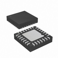
Manufacturer Part Number
ATTINY48-MMU
Description
MCU AVR 5K FLASH 12MHZ 28-QFN
Manufacturer
Atmel
Series
AVR® ATtinyr
Specifications of ATTINY48-MMU
Core Processor
AVR
Core Size
8-Bit
Speed
12MHz
Connectivity
I²C, SPI
Peripherals
Brown-out Detect/Reset, POR, WDT
Number Of I /o
24
Program Memory Size
4KB (2K x 16)
Program Memory Type
FLASH
Eeprom Size
64 x 8
Ram Size
256 x 8
Voltage - Supply (vcc/vdd)
1.8 V ~ 5.5 V
Data Converters
A/D 6x10b
Oscillator Type
Internal
Operating Temperature
-40°C ~ 85°C
Package / Case
28-VQFN Exposed Pad, 28-HVQFN, 28-SQFN, 28-DHVQFN
Processor Series
ATTINY4x
Core
AVR8
Data Bus Width
8 bit
Data Ram Size
256 B
Interface Type
2-Wire, I2S, SPI
Maximum Clock Frequency
12 MHz
Number Of Programmable I/os
24
Number Of Timers
2
Maximum Operating Temperature
+ 85 C
Mounting Style
SMD/SMT
3rd Party Development Tools
EWAVR, EWAVR-BL
Development Tools By Supplier
ATAVRDRAGON, ATSTK500, ATSTK600, ATAVRISP2, ATAVRONEKIT
Minimum Operating Temperature
- 40 C
On-chip Adc
10 bit, 6 Channel
Package
28VQFN EP
Device Core
AVR
Family Name
ATtiny
Maximum Speed
12 MHz
Operating Supply Voltage
2.5|3.3|5 V
For Use With
ATAVRDRAGON - KIT DRAGON 32KB FLASH MEM AVR
Lead Free Status / RoHS Status
Lead free / RoHS Compliant


92
ATtiny48/88
It is important to notice that accessing 16-bit registers are atomic operations. If an interrupt
occurs between the two instructions accessing the 16-bit register, and the interrupt code
updates the temporary register by accessing the same or any other of the 16-bit Timer Regis-
ters, then the result of the access outside the interrupt will be corrupted. Therefore, when both
the main code and the interrupt code update the temporary register, the main code must disable
the interrupts during the 16-bit access.
The following code examples show how to do an atomic read of the TCNT1 Register contents.
Reading any of the OCR1A/B or ICR1 Registers can be done by using the same principle.
Note:
The assembly code example returns the TCNT1 value in the r17:r16 register pair.
Assembly Code Example
C Code Example
TIM16_ReadTCNT1:
unsigned int TIM16_ReadTCNT1( void )
{
}
; Save global interrupt flag
in r18,SREG
; Disable interrupts
cli
; Read TCNT1 into r17:r16
in r16,TCNT1L
in r17,TCNT1H
; Restore global interrupt flag
out SREG,r18
ret
unsigned char sreg;
unsigned int i;
/* Save global interrupt flag */
sreg = SREG;
/* Disable interrupts */
_CLI();
/* Read TCNT1 into i */
i = TCNT1;
/* Restore global interrupt flag */
SREG = sreg;
return i;
1.
See ”About Code Examples” on page 7.
For I/O Registers located in extended I/O map, “IN”, “OUT”, “SBIS”, “SBIC”, “CBI”, and “SBI”
instructions must be replaced with instructions that allow access to extended I/O. Typically
“LDS” and “STS” combined with “SBRS”, “SBRC”, “SBR”, and “CBR”.
(1)
(1)
8008G–AVR–04/11
Related parts for ATTINY48-MMU
Image
Part Number
Description
Manufacturer
Datasheet
Request
R

Part Number:
Description:
Manufacturer:
Atmel Corporation
Datasheet:

Part Number:
Description:
MCU AVR 4K ISP FLASH 1.8V 32TQFP
Manufacturer:
Atmel
Datasheet:

Part Number:
Description:
MCU AVR 4K ISP FLASH 1.8V 32-QFN
Manufacturer:
Atmel
Datasheet:

Part Number:
Description:
MCU AVR 4K ISP FLASH 1.8V 28-DIP
Manufacturer:
Atmel
Datasheet:

Part Number:
Description:
MCU AVR 4KB FLASH 12MHZ 32TQFP
Manufacturer:
Atmel
Datasheet:
Part Number:
Description:
MCU AVR 4KB FLASH 12MHZ 32QFN
Manufacturer:
Atmel
Datasheet:

Part Number:
Description:
MCU AVR 4KB FLASH 12MHZ 28-VQFN
Manufacturer:
Atmel
Datasheet:
Part Number:
Description:
MCU AVR 4KB FLASH 12MHZ 28QFN
Manufacturer:
Atmel
Datasheet:
Part Number:
Description:
8-bit Microcontrollers - MCU 4KB FL,64B EE, 256B SRAM-12MHz
Manufacturer:
Atmel
Part Number:
Description:
8-bit Microcontrollers - MCU Microcontroller
Manufacturer:
Atmel
Part Number:
Description:
Manufacturer:
Atmel Corporation
Datasheet: