ATTINY48-MMU Atmel, ATTINY48-MMU Datasheet - Page 198
ATTINY48-MMU
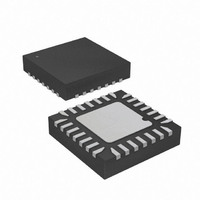
Manufacturer Part Number
ATTINY48-MMU
Description
MCU AVR 5K FLASH 12MHZ 28-QFN
Manufacturer
Atmel
Series
AVR® ATtinyr
Specifications of ATTINY48-MMU
Core Processor
AVR
Core Size
8-Bit
Speed
12MHz
Connectivity
I²C, SPI
Peripherals
Brown-out Detect/Reset, POR, WDT
Number Of I /o
24
Program Memory Size
4KB (2K x 16)
Program Memory Type
FLASH
Eeprom Size
64 x 8
Ram Size
256 x 8
Voltage - Supply (vcc/vdd)
1.8 V ~ 5.5 V
Data Converters
A/D 6x10b
Oscillator Type
Internal
Operating Temperature
-40°C ~ 85°C
Package / Case
28-VQFN Exposed Pad, 28-HVQFN, 28-SQFN, 28-DHVQFN
Processor Series
ATTINY4x
Core
AVR8
Data Bus Width
8 bit
Data Ram Size
256 B
Interface Type
2-Wire, I2S, SPI
Maximum Clock Frequency
12 MHz
Number Of Programmable I/os
24
Number Of Timers
2
Maximum Operating Temperature
+ 85 C
Mounting Style
SMD/SMT
3rd Party Development Tools
EWAVR, EWAVR-BL
Development Tools By Supplier
ATAVRDRAGON, ATSTK500, ATSTK600, ATAVRISP2, ATAVRONEKIT
Minimum Operating Temperature
- 40 C
On-chip Adc
10 bit, 6 Channel
Package
28VQFN EP
Device Core
AVR
Family Name
ATtiny
Maximum Speed
12 MHz
Operating Supply Voltage
2.5|3.3|5 V
For Use With
ATAVRDRAGON - KIT DRAGON 32KB FLASH MEM AVR
Lead Free Status / RoHS Status
Lead free / RoHS Compliant


21.2.7
21.2.8
21.2.9
21.2.10
198
ATtiny48/88
Reading the EEPROM
Programming Low Fuse Bits
Programming High Fuse Bits
Programming Extended Fuse Bits
The algorithm for reading the EEPROM memory is as follows (see
page 194
The algorithm for programming the low fuse bits is as follows (see
page 194
The algorithm for programming the high fuse bits is as follows (see
page 194
The algorithm for programming the extended fuse bits is as follows (see
Flash” on page 194
EEPROM programming waveforms are illustrated in
and letters refer to the programming steps described above.
• Set BS1 to “1”. The Flash word high byte can now be read at DATA
• Set OE to “1”
• A: Load command “0000 0011”
• G: Load address high byte (0x00 – 0xFF)
• B: Load address low byte (0x00 – 0xFF)
• Set OE to “0”, and BS1 to “0”. The EEPROM Data byte can now be read at DATA
• Set OE to “1”
• A: Load command “0100 0000”
• C: Load data low byte. Bit n = “0” programs and bit n = “1” erases the fuse bit
• Give WR a negative pulse and wait for RDY/BSY to go high
• A: Load command “0100 0000”
• C: Load data low byte. Bit n = “0” programs and bit n = “1” erases the fuse bit
• Set BS1 to “1” and BS2 to “0”. This selects high data byte
• Give WR a negative pulse and wait for RDY/BSY to go high
• Set BS1 to “0”. This selects low data byte
• A: Load command “0100 0000”
• C: Load data low byte. Bit n = “0” programs and bit n = “1” erases the fuse bit
• Set BS1 to “0” and BS2 to “1”. This selects extended data byte
• Give WR a negative pulse and wait for RDY/BSY to go high
• Set BS2 to “0”. This selects low data byte
for details on command and address loading):
for details on command and data loading):
for details on command and data loading):
for details on command and data loading):
Figure
21-5, where XX means “don’t care”
“Programming the Flash” on
“Programming the Flash” on
“Programming the Flash” on
“Programming the
8008G–AVR–04/11
Related parts for ATTINY48-MMU
Image
Part Number
Description
Manufacturer
Datasheet
Request
R

Part Number:
Description:
Manufacturer:
Atmel Corporation
Datasheet:

Part Number:
Description:
MCU AVR 4K ISP FLASH 1.8V 32TQFP
Manufacturer:
Atmel
Datasheet:

Part Number:
Description:
MCU AVR 4K ISP FLASH 1.8V 32-QFN
Manufacturer:
Atmel
Datasheet:

Part Number:
Description:
MCU AVR 4K ISP FLASH 1.8V 28-DIP
Manufacturer:
Atmel
Datasheet:

Part Number:
Description:
MCU AVR 4KB FLASH 12MHZ 32TQFP
Manufacturer:
Atmel
Datasheet:
Part Number:
Description:
MCU AVR 4KB FLASH 12MHZ 32QFN
Manufacturer:
Atmel
Datasheet:

Part Number:
Description:
MCU AVR 4KB FLASH 12MHZ 28-VQFN
Manufacturer:
Atmel
Datasheet:
Part Number:
Description:
MCU AVR 4KB FLASH 12MHZ 28QFN
Manufacturer:
Atmel
Datasheet:
Part Number:
Description:
8-bit Microcontrollers - MCU 4KB FL,64B EE, 256B SRAM-12MHz
Manufacturer:
Atmel
Part Number:
Description:
8-bit Microcontrollers - MCU Microcontroller
Manufacturer:
Atmel
Part Number:
Description:
Manufacturer:
Atmel Corporation
Datasheet: