ATTINY48-MMU Atmel, ATTINY48-MMU Datasheet - Page 19
ATTINY48-MMU
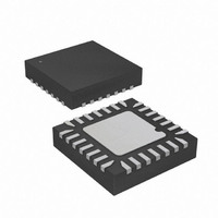
Manufacturer Part Number
ATTINY48-MMU
Description
MCU AVR 5K FLASH 12MHZ 28-QFN
Manufacturer
Atmel
Series
AVR® ATtinyr
Specifications of ATTINY48-MMU
Core Processor
AVR
Core Size
8-Bit
Speed
12MHz
Connectivity
I²C, SPI
Peripherals
Brown-out Detect/Reset, POR, WDT
Number Of I /o
24
Program Memory Size
4KB (2K x 16)
Program Memory Type
FLASH
Eeprom Size
64 x 8
Ram Size
256 x 8
Voltage - Supply (vcc/vdd)
1.8 V ~ 5.5 V
Data Converters
A/D 6x10b
Oscillator Type
Internal
Operating Temperature
-40°C ~ 85°C
Package / Case
28-VQFN Exposed Pad, 28-HVQFN, 28-SQFN, 28-DHVQFN
Processor Series
ATTINY4x
Core
AVR8
Data Bus Width
8 bit
Data Ram Size
256 B
Interface Type
2-Wire, I2S, SPI
Maximum Clock Frequency
12 MHz
Number Of Programmable I/os
24
Number Of Timers
2
Maximum Operating Temperature
+ 85 C
Mounting Style
SMD/SMT
3rd Party Development Tools
EWAVR, EWAVR-BL
Development Tools By Supplier
ATAVRDRAGON, ATSTK500, ATSTK600, ATAVRISP2, ATAVRONEKIT
Minimum Operating Temperature
- 40 C
On-chip Adc
10 bit, 6 Channel
Package
28VQFN EP
Device Core
AVR
Family Name
ATtiny
Maximum Speed
12 MHz
Operating Supply Voltage
2.5|3.3|5 V
For Use With
ATAVRDRAGON - KIT DRAGON 32KB FLASH MEM AVR
Lead Free Status / RoHS Status
Lead free / RoHS Compliant


5.2.3
5.2.4
8008G–AVR–04/11
Extended I/O Register File
Data Memory (SRAM)
ATtiny48/88 also contains three general purpose I/O registers that can be used for storing any
information. See GPIOR0, GPIOR1 and GPIOR2 in
general purpose I/O registers are particularly useful for storing global variables and status flags,
since they are accessible to bit-specific instructions such as SBI, CBI, SBIC, SBIS, SBRC, and
SBRS.
Following the standard I/O register file, the next
isters. ATtiny48/88 is a complex microcontroller with more peripheral units than can be
addressed with the IN and OUT instructions. Registers in the extended I/O area must be
accessed using instructions LD/LDD/LDI/LDS and ST/STD/STS. See
on page
See
Following the general purpose register file and the I/O register files, the remaining
tions are reserved for the internal data SRAM.
There are five addressing modes available:
All addressing modes can be used on the entire volatile memory, including the general purpose
register file, the I/O register files and the data memory.
Internal SRAM is accessed in two clk
• Direct. This mode of addressing reaches the entire data space.
• Indirect.
• Indirect with Displacement. This mode of addressing reaches 63 address locations from the
• Indirect with Pre-decrement. In this mode the address register is automatically decremented
• Indirect with Post-increment. In this mode the address register is automatically incremented
base address given by the Y- or Z-register.
before access. Address pointer registers (X, Y, and Z) are located in the general purpose
register file, in registers R26 to R31. See
after access. Address pointer registers (X, Y, and Z) are located in the general purpose
register file, in registers R26 to R31. See
“Register Summary” on page 277
281.
CPU
for a list of I/O registers.
cycles, as illustrated in
“General Purpose Register File” on page
“General Purpose Register File” on page
160
locations are reserved for extended I/O reg-
“Register Summary” on page
Figure
“Instruction Set Summary”
5-2, below.
ATtiny48/88
256/512
277. These
10.
10.
loca-
19
Related parts for ATTINY48-MMU
Image
Part Number
Description
Manufacturer
Datasheet
Request
R

Part Number:
Description:
Manufacturer:
Atmel Corporation
Datasheet:

Part Number:
Description:
MCU AVR 4K ISP FLASH 1.8V 32TQFP
Manufacturer:
Atmel
Datasheet:

Part Number:
Description:
MCU AVR 4K ISP FLASH 1.8V 32-QFN
Manufacturer:
Atmel
Datasheet:

Part Number:
Description:
MCU AVR 4K ISP FLASH 1.8V 28-DIP
Manufacturer:
Atmel
Datasheet:

Part Number:
Description:
MCU AVR 4KB FLASH 12MHZ 32TQFP
Manufacturer:
Atmel
Datasheet:
Part Number:
Description:
MCU AVR 4KB FLASH 12MHZ 32QFN
Manufacturer:
Atmel
Datasheet:

Part Number:
Description:
MCU AVR 4KB FLASH 12MHZ 28-VQFN
Manufacturer:
Atmel
Datasheet:
Part Number:
Description:
MCU AVR 4KB FLASH 12MHZ 28QFN
Manufacturer:
Atmel
Datasheet:
Part Number:
Description:
8-bit Microcontrollers - MCU 4KB FL,64B EE, 256B SRAM-12MHz
Manufacturer:
Atmel
Part Number:
Description:
8-bit Microcontrollers - MCU Microcontroller
Manufacturer:
Atmel
Part Number:
Description:
Manufacturer:
Atmel Corporation
Datasheet: