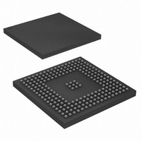
AT91SAM9260B-CU-999 Atmel, AT91SAM9260B-CU-999 Datasheet - Page 549

AT91SAM9260B-CU-999
Manufacturer Part Number
AT91SAM9260B-CU-999
Description
IC MCU ARM9 217LFBGA
Manufacturer
Atmel
Series
AT91SAMr
Datasheet
1.AT91SAM9260B-CU-999.pdf
(798 pages)
Specifications of AT91SAM9260B-CU-999
Core Processor
ARM9
Core Size
16/32-Bit
Speed
180MHz
Connectivity
EBI/EMI, Ethernet, I²C, MMC, SPI, SSC, UART/USART, USB
Peripherals
POR, WDT
Number Of I /o
96
Program Memory Size
32KB (32K x 8)
Program Memory Type
ROM
Ram Size
24K x 8
Voltage - Supply (vcc/vdd)
1.65 V ~ 1.95 V
Data Converters
A/D 4x10b
Oscillator Type
Internal
Operating Temperature
-40°C ~ 85°C
Package / Case
217-LFBGA
Processor Series
AT91SAMx
Core
ARM926EJ-S
Data Bus Width
32 bit
Data Ram Size
8 KB
Interface Type
2-Wire, EBI, I2S, SPI, USART
Maximum Clock Frequency
180 MHz
Number Of Programmable I/os
96
Number Of Timers
6
Maximum Operating Temperature
+ 85 C
Mounting Style
SMD/SMT
3rd Party Development Tools
JTRACE-ARM-2M, MDK-ARM, RL-ARM, ULINK2
Development Tools By Supplier
AT91SAM-ICE, AT91-ISP, AT91SAM9260-EK
Minimum Operating Temperature
- 40 C
On-chip Adc
10 bit, 4 Channel
For Use With
AT91SAM9260-EK - KIT EVAL FOR AT91SAM9260AT91SAM-ICE - EMULATOR FOR AT91 ARM7/ARM9
Lead Free Status / RoHS Status
Lead free / RoHS Compliant
Eeprom Size
-
Lead Free Status / Rohs Status
Details
Available stocks
Company
Part Number
Manufacturer
Quantity
Price
- Current page: 549 of 798
- Download datasheet (12Mb)
34.4
Figure 34-2. Application Block Diagram
34.5
Table 34-1.
Notes:
34.6
34.6.1
6221I–ATARM–17-Jul-09
Pin Name
MCCDA/MCCDB
MCCK
MCDA0 - MCDA3
MCDB0 - MCDB3
Application Block Diagram
Pin Name List
1. I: Input, O: Output, PP: Push/Pull, OD: Open Drain.
2. When several MCI (x MCI) are embedded in a product, MCCK refers to MCIx_CK, MCCDA to MCIx_CDA, MCCDB to
Product Dependencies
I/O Lines
(2)
MCIx_CDB, MCDAy to MCIx_DAy, MCDBy to MCIx_DBy.
I/O Lines Description
The pins used for interfacing the MultiMedia Cards or SD Cards may be multiplexed with PIO
lines. The programmer must first program the PIO controllers to assign the peripheral functions
to MCI pins.
Pin Description
Command/response
Clock
Data 0..3 of Slot A
Data 0..3 of Slot B
1
2 3 4 5 6
ex: File System, Audio, Security, etc.
MMC
7
Application Layer
Physical Layer
MCI Interface
9
1
2 3 4 5 6
Type
I/O/PP/OD
I/O
I/O/PP
I/O/PP
SDCard
(1)
7 8
Comments
CMD of an MMC or SDCard/SDIO
CLK of an MMC or SD Card/SDIO
DAT0 of an MMC
DAT[0..3] of an SD Card/SDIO
DAT0 of an MMC
DAT[0..3] of an SD Card/SDIO
AT91SAM9260
549
Related parts for AT91SAM9260B-CU-999
Image
Part Number
Description
Manufacturer
Datasheet
Request
R

Part Number:
Description:
Manufacturer:
ATMEL Corporation
Datasheet:

Part Number:
Description:
KIT EVAL FOR AT91SAM9260
Manufacturer:
Atmel
Datasheet:

Part Number:
Description:
AT91 ARM Thumb Microcontrollers
Manufacturer:
ATMEL [ATMEL Corporation]
Datasheet:

Part Number:
Description:
AT91 ARM Thumb Microcontrollers
Manufacturer:
ATMEL Corporation
Datasheet:

Part Number:
Description:
At91 Arm Thumb Microcontrollers
Manufacturer:
ATMEL Corporation
Datasheet:

Part Number:
Description:
MCU, MPU & DSP Development Tools DEV BRD FOR AT91SAM9260
Manufacturer:
Olimex Ltd.
Datasheet:

Part Number:
Description:
MCU, MPU & DSP Development Tools KICKSTART KIT FOR AT91SAM9 PLUS
Manufacturer:
IAR Systems

Part Number:
Description:
DEV KIT FOR AVR/AVR32
Manufacturer:
Atmel
Datasheet:

Part Number:
Description:
INTERVAL AND WIPE/WASH WIPER CONTROL IC WITH DELAY
Manufacturer:
ATMEL Corporation
Datasheet:

Part Number:
Description:
Low-Voltage Voice-Switched IC for Hands-Free Operation
Manufacturer:
ATMEL Corporation
Datasheet:

Part Number:
Description:
MONOLITHIC INTEGRATED FEATUREPHONE CIRCUIT
Manufacturer:
ATMEL Corporation
Datasheet:

Part Number:
Description:
AM-FM Receiver IC U4255BM-M
Manufacturer:
ATMEL Corporation
Datasheet:

Part Number:
Description:
Monolithic Integrated Feature Phone Circuit
Manufacturer:
ATMEL Corporation
Datasheet:

Part Number:
Description:
Multistandard Video-IF and Quasi Parallel Sound Processing
Manufacturer:
ATMEL Corporation
Datasheet:


