AT91SAM9260B-CU-999 Atmel, AT91SAM9260B-CU-999 Datasheet - Page 764
AT91SAM9260B-CU-999
Manufacturer Part Number
AT91SAM9260B-CU-999
Description
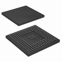
IC MCU ARM9 217LFBGA
Manufacturer
Atmel
Series
AT91SAMr
Datasheet
1.AT91SAM9260B-CU-999.pdf
(798 pages)
Specifications of AT91SAM9260B-CU-999
Core Processor
ARM9
Core Size
16/32-Bit
Speed
180MHz
Connectivity
EBI/EMI, Ethernet, I²C, MMC, SPI, SSC, UART/USART, USB
Peripherals
POR, WDT
Number Of I /o
96
Program Memory Size
32KB (32K x 8)
Program Memory Type
ROM
Ram Size
24K x 8
Voltage - Supply (vcc/vdd)
1.65 V ~ 1.95 V
Data Converters
A/D 4x10b
Oscillator Type
Internal
Operating Temperature
-40°C ~ 85°C
Package / Case
217-LFBGA
Processor Series
AT91SAMx
Core
ARM926EJ-S
Data Bus Width
32 bit
Data Ram Size
8 KB
Interface Type
2-Wire, EBI, I2S, SPI, USART
Maximum Clock Frequency
180 MHz
Number Of Programmable I/os
96
Number Of Timers
6
Maximum Operating Temperature
+ 85 C
Mounting Style
SMD/SMT
3rd Party Development Tools
JTRACE-ARM-2M, MDK-ARM, RL-ARM, ULINK2
Development Tools By Supplier
AT91SAM-ICE, AT91-ISP, AT91SAM9260-EK
Minimum Operating Temperature
- 40 C
On-chip Adc
10 bit, 4 Channel
For Use With
AT91SAM9260-EK - KIT EVAL FOR AT91SAM9260AT91SAM-ICE - EMULATOR FOR AT91 ARM7/ARM9
Lead Free Status / RoHS Status
Lead free / RoHS Compliant
Eeprom Size
-
Lead Free Status / Rohs Status
Details
Available stocks
Company
Part Number
Manufacturer
Quantity
Price


43.2.11.2
43.2.11.3
43.2.11.4
43.2.12
43.2.12.1
764
AT91SAM9260
Static Memory Controller (SMC)
Incorrect first RK Clock Cycle when RK Outputs a Clock During Data Transfer
Transmitter Limitations in Slave Mode
Periodic Transmission Limitations in Master Mode
SMC: Chip Select Parameters Modification
then, at the end of the data, the RK pin is set in high impedance which may be interpreted as an
unexpected clock cycle.
Enable the pull-up on RK pin.
When the SSC receiver is used in the following configuration:
then the first clock cycle time generated by the RK pin is equal to MCK/(2 x (DIV +1)) instead of
MCK/(2 x DIV).
None.
If TK is programmed as output and TF is programmed as input, it is impossible to emit data
when start of edge (rising or falling) of synchro has a Start Delay equal to zero.
None.
If Least Significant Bit is sent first (MSBF = 0) the first TAG during the frame synchro is not sent.
None.
The user must not change the configuration parameters of an SMC Chip Select (Setup, Pulse,
Cycle, Mode) if accesses are performed on this CS during the modification.
For example, the modification of the Chip Select 0 (CS0) parameters, while fetching the code
from a memory connected on this CS0, may lead to unpredictable behavior.
The code used to modify the parameters of an SMC Chip Select can be executed from the inter-
nal RAM or from a memory connected to another Chip Select.
• data sampled on RK falling edge (CKI = 0)
• RX clock is divided clock (CKS = 0 and DIV different from 0)
• RK pin set as output and provides the clock during data transfer (CKO = 2)
• data sampled on RK falling edge (CKI = 0)
Problem Fix/Workaround
Problem Fix/Workaround
Problem Fix/Workaround
Problem Fix/Workaround
Problem Fix/Workaround
6221I–ATARM–17-Jul-09
Related parts for AT91SAM9260B-CU-999
Image
Part Number
Description
Manufacturer
Datasheet
Request
R

Part Number:
Description:
Manufacturer:
ATMEL Corporation
Datasheet:

Part Number:
Description:
KIT EVAL FOR AT91SAM9260
Manufacturer:
Atmel
Datasheet:

Part Number:
Description:
AT91 ARM Thumb Microcontrollers
Manufacturer:
ATMEL [ATMEL Corporation]
Datasheet:
Part Number:
Description:
AT91 ARM Thumb Microcontrollers
Manufacturer:
ATMEL Corporation
Datasheet:
Part Number:
Description:
At91 Arm Thumb Microcontrollers
Manufacturer:
ATMEL Corporation
Datasheet:

Part Number:
Description:
MCU, MPU & DSP Development Tools DEV BRD FOR AT91SAM9260
Manufacturer:
Olimex Ltd.
Datasheet:

Part Number:
Description:
MCU, MPU & DSP Development Tools KICKSTART KIT FOR AT91SAM9 PLUS
Manufacturer:
IAR Systems

Part Number:
Description:
DEV KIT FOR AVR/AVR32
Manufacturer:
Atmel
Datasheet:
Part Number:
Description:
INTERVAL AND WIPE/WASH WIPER CONTROL IC WITH DELAY
Manufacturer:
ATMEL Corporation
Datasheet:
Part Number:
Description:
Low-Voltage Voice-Switched IC for Hands-Free Operation
Manufacturer:
ATMEL Corporation
Datasheet:
Part Number:
Description:
MONOLITHIC INTEGRATED FEATUREPHONE CIRCUIT
Manufacturer:
ATMEL Corporation
Datasheet:
Part Number:
Description:
AM-FM Receiver IC U4255BM-M
Manufacturer:
ATMEL Corporation
Datasheet:
Part Number:
Description:
Monolithic Integrated Feature Phone Circuit
Manufacturer:
ATMEL Corporation
Datasheet:
Part Number:
Description:
Multistandard Video-IF and Quasi Parallel Sound Processing
Manufacturer:
ATMEL Corporation
Datasheet: