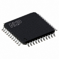
P89V662FBC,557 NXP Semiconductors, P89V662FBC,557 Datasheet - Page 29

P89V662FBC,557
Manufacturer Part Number
P89V662FBC,557
Description
IC 80C51 MCU FLASH 32K 44-TQFP
Manufacturer
NXP Semiconductors
Series
89Vr
Datasheet
1.P89V660FBC557.pdf
(89 pages)
Specifications of P89V662FBC,557
Program Memory Type
FLASH
Program Memory Size
32KB (32K x 8)
Package / Case
44-TQFP
Core Processor
8051
Core Size
8-Bit
Speed
40MHz
Connectivity
I²C, SPI, UART/USART
Peripherals
POR, PWM, WDT
Number Of I /o
36
Ram Size
1K x 8
Voltage - Supply (vcc/vdd)
4.5 V ~ 5.5 V
Oscillator Type
Internal
Operating Temperature
-40°C ~ 85°C
Processor Series
P89V6x
Core
80C51
Data Bus Width
8 bit
Data Ram Size
1 KB
Interface Type
I2C/UART
Maximum Clock Frequency
40 MHz
Number Of Programmable I/os
36
Number Of Timers
3
Operating Supply Voltage
4.5 V to 5.5 V
Maximum Operating Temperature
+ 85 C
Mounting Style
SMD/SMT
3rd Party Development Tools
PK51, CA51, A51, ULINK2
Minimum Operating Temperature
- 40 C
Lead Free Status / RoHS Status
Lead free / RoHS Compliant
For Use With
622-1001 - USB IN-CIRCUIT PROG 80C51ISP
Eeprom Size
-
Data Converters
-
Lead Free Status / Rohs Status
Lead free / RoHS Compliant
Other names
568-2435
935280832557
P89V662FBC
935280832557
P89V662FBC
Available stocks
Company
Part Number
Manufacturer
Quantity
Price
Company:
Part Number:
P89V662FBC,557
Manufacturer:
Maxim
Quantity:
260
Company:
Part Number:
P89V662FBC,557
Manufacturer:
NXP Semiconductors
Quantity:
10 000
NXP Semiconductors
P89V660_662_664_3
Product data sheet
6.4.5.2 Master receiver mode
The I
will send the START condition as soon as the bus is free. After the START condition is
transmitted, the SI bit is set, and the status code in S1STA should be 08H. This status
code must be used to vector to an interrupt service routine where the user should load the
slave address to S1DAT and data direction bit (SLA+W). The SI bit must be cleared before
the data transfer can continue.
When the slave address and R/W bit have been transmitted and an acknowledgment bit
has been received, the SI bit is set again, and the possible status codes are 18H, 20H, or
38H for the master mode or 68H, 78H, or 0B0H if the slave mode was enabled (setting
AA = Logic 1). The appropriate action to be taken for each of these status codes is shown
in
In the Master Receiver mode, data is received from a slave transmitter. The transfer
started in the same manner as in the Master Transmitter mode. When the START
condition has been transmitted, the interrupt service routine must load the slave address
and the data direction bit to I
before the data transfer can continue.
When the slave address and data direction bit have been transmitted and an acknowledge
bit has been received, the SI bit is set, and the Status Register will show the status code.
For master mode, the possible status codes are 40H, 48H, or 38H. For slave mode, the
possible status codes are 68H, 78H, or B0H. Refer to
After a repeated START condition, I
Fig 8. Format in the Master Transmitter mode
Fig 9. Format of Master Receiver mode
Table
2
C-bus will enter Master Transmitter mode by setting the STA bit. The I
22.
from master to slave
from slave to master
from master to slave
from slave to master
S
S
Rev. 03 — 10 November 2008
slave address
slave address
2
C-bus Data Register (S1DAT). The SI bit must be cleared
logic 0 = write
logic 1 = read
logic 0 = write
logic 1 = read
80C51 with 512 B/1 kB/2 kB RAM, dual I
2
R/W
C-bus may switch to the Master Transmitter mode.
R
A
A
A = acknowledge (SDA LOW)
A = not acknowledge (SDA HIGH)
S = START condition
A = acknowledge (SDA LOW)
A = not acknowledge (SDA HIGH)
S = START condition
P = STOP condition
DATA
DATA
(n Bytes + acknowledge)
(n Bytes + acknowledge)
data transferred
data transferred
A
A
P89V660/662/664
Table 24
DATA
DATA
for details.
A/A
A
002aaa929
002aaa930
P
P
© NXP B.V. 2008. All rights reserved.
2
C-bus logic
2
C-bus, SPI
29 of 89


