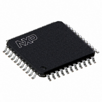
P89V662FBC,557 NXP Semiconductors, P89V662FBC,557 Datasheet - Page 50

P89V662FBC,557
Manufacturer Part Number
P89V662FBC,557
Description
IC 80C51 MCU FLASH 32K 44-TQFP
Manufacturer
NXP Semiconductors
Series
89Vr
Datasheet
1.P89V660FBC557.pdf
(89 pages)
Specifications of P89V662FBC,557
Program Memory Type
FLASH
Program Memory Size
32KB (32K x 8)
Package / Case
44-TQFP
Core Processor
8051
Core Size
8-Bit
Speed
40MHz
Connectivity
I²C, SPI, UART/USART
Peripherals
POR, PWM, WDT
Number Of I /o
36
Ram Size
1K x 8
Voltage - Supply (vcc/vdd)
4.5 V ~ 5.5 V
Oscillator Type
Internal
Operating Temperature
-40°C ~ 85°C
Processor Series
P89V6x
Core
80C51
Data Bus Width
8 bit
Data Ram Size
1 KB
Interface Type
I2C/UART
Maximum Clock Frequency
40 MHz
Number Of Programmable I/os
36
Number Of Timers
3
Operating Supply Voltage
4.5 V to 5.5 V
Maximum Operating Temperature
+ 85 C
Mounting Style
SMD/SMT
3rd Party Development Tools
PK51, CA51, A51, ULINK2
Minimum Operating Temperature
- 40 C
Lead Free Status / RoHS Status
Lead free / RoHS Compliant
For Use With
622-1001 - USB IN-CIRCUIT PROG 80C51ISP
Eeprom Size
-
Data Converters
-
Lead Free Status / Rohs Status
Lead free / RoHS Compliant
Other names
568-2435
935280832557
P89V662FBC
935280832557
P89V662FBC
Available stocks
Company
Part Number
Manufacturer
Quantity
Price
Company:
Part Number:
P89V662FBC,557
Manufacturer:
Maxim
Quantity:
260
Company:
Part Number:
P89V662FBC,557
Manufacturer:
NXP Semiconductors
Quantity:
10 000
NXP Semiconductors
P89V660_662_664_3
Product data sheet
6.7.5 Framing error
6.7.6 More about UART mode 1
6.7.7 More about UART modes 2 and 3
Table 38.
Table 39.
Framing error (FE) is reported in the SCON.7 bit if SMOD0 (PCON.6) = 1. If SMOD0 = 0,
SCON.7 is the SM0 bit for the UART, it is recommended that SM0 is set up before SMOD0
is set to ‘1’.
Reception is initiated by a detected 1-to-0 transition at RXD. For this purpose RXD is
sampled at a rate of 16 times whatever baud rate has been established. When a transition
is detected, the divide-by-16 counter is immediately reset to align its rollovers with the
boundaries of the incoming bit times.
The 16 states of the counter divide each bit time into 16ths. At the 7th, 8th, and 9th
counter states of each bit time, the bit detector samples the value of RXD. The value
accepted is the value that was seen in at least 2 of the 3 samples. This is done for noise
rejection. If the value accepted during the first bit time is not 0, the receive circuits are
reset and the unit goes back to looking for another 1-to-0 transition. This is to provide
rejection of false start bits. If the start bit proves valid, it is shifted into the input shift
register, and reception of the rest of the frame will proceed.
The signal to load SBUF and RB8, and to set RI, will be generated if, and only if, the
following conditions are met at the time the final shift pulse is generated: (a) RI = 0, and
(b) Either SM2 = 0, or the received stop bit = 1.
If either of these two conditions is not met, the received frame is irretrievably lost. If both
conditions are met, the stop bit goes into RB8, the 8 data bits go into SBUF, and RI is
activated.
Reception is performed in the same manner as in mode 1.
Bit
3
2
1
0
SM0, SM1
0 0
0 1
1 0
1 1
SCON - Serial port control register (address 98H) bit description
SCON - Serial port control register (address 98H) SM0/SM1 mode definition
Symbol
TB8
RB8
TI
RI
UART mode
0: shift register
1: 8-bit UART
2: 9-bit UART
3: 9-bit UART
Rev. 03 — 10 November 2008
Description
The 9th data bit that will be transmitted in Modes 2 and 3. Set or clear
by software as desired.
In Modes 2 and 3, is the 9th data bit that was received. In Mode 1, it
SM2 = 0, RB8 is the stop bit that was received. In Mode 0, RB8 is
undefined.
Transmit interrupt flag. Set by hardware at the end of the 8th bit time in
Mode 0, or at the stop bit in the other modes, in any serial
transmission. Must be cleared by software.
Receive interrupt flag. Set by hardware at the end of the 8th bit time in
Mode 0, or approximately halfway through the stop bit time in all other
modes. (See SM2 for exceptions). Must be cleared by software.
80C51 with 512 B/1 kB/2 kB RAM, dual I
Baud rate
CPU clock / 6
variable
CPU clock / 32 or CPU clock / 16
variable
P89V660/662/664
© NXP B.V. 2008. All rights reserved.
…continued
2
C-bus, SPI
50 of 89


