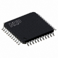
P89V662FBC,557 NXP Semiconductors, P89V662FBC,557 Datasheet - Page 78

P89V662FBC,557
Manufacturer Part Number
P89V662FBC,557
Description
IC 80C51 MCU FLASH 32K 44-TQFP
Manufacturer
NXP Semiconductors
Series
89Vr
Datasheet
1.P89V660FBC557.pdf
(89 pages)
Specifications of P89V662FBC,557
Program Memory Type
FLASH
Program Memory Size
32KB (32K x 8)
Package / Case
44-TQFP
Core Processor
8051
Core Size
8-Bit
Speed
40MHz
Connectivity
I²C, SPI, UART/USART
Peripherals
POR, PWM, WDT
Number Of I /o
36
Ram Size
1K x 8
Voltage - Supply (vcc/vdd)
4.5 V ~ 5.5 V
Oscillator Type
Internal
Operating Temperature
-40°C ~ 85°C
Processor Series
P89V6x
Core
80C51
Data Bus Width
8 bit
Data Ram Size
1 KB
Interface Type
I2C/UART
Maximum Clock Frequency
40 MHz
Number Of Programmable I/os
36
Number Of Timers
3
Operating Supply Voltage
4.5 V to 5.5 V
Maximum Operating Temperature
+ 85 C
Mounting Style
SMD/SMT
3rd Party Development Tools
PK51, CA51, A51, ULINK2
Minimum Operating Temperature
- 40 C
Lead Free Status / RoHS Status
Lead free / RoHS Compliant
For Use With
622-1001 - USB IN-CIRCUIT PROG 80C51ISP
Eeprom Size
-
Data Converters
-
Lead Free Status / Rohs Status
Lead free / RoHS Compliant
Other names
568-2435
935280832557
P89V662FBC
935280832557
P89V662FBC
Available stocks
Company
Part Number
Manufacturer
Quantity
Price
Company:
Part Number:
P89V662FBC,557
Manufacturer:
Maxim
Quantity:
260
Company:
Part Number:
P89V662FBC,557
Manufacturer:
NXP Semiconductors
Quantity:
10 000
NXP Semiconductors
Table 74.
[1]
[2]
[3]
P89V660_662_664_3
Product data sheet
Symbol
t
t
t
t
t
t
t
t
t
t
t
t
t
t
HD;STA
LOW
HIGH
r(SCL)
f(SCL)
SU;DAT
suDAT1
suDAT2
HD;DAT
SU;STA
SU;STO
BUF
r(SDA)
f(SDA)
Fig 40. Shift register mode timing waveforms
At 100 kb/s. All other bit rates, this value is inversely proportional to the bit rate of 100 kb/s.
Determined by the external bus capacitance and pull-up resistor. This must be < 1 s.
Spikes on SDA and SCL with a duration less than 3T
write to SBUF
output data
I
2
instruction
input data
C-bus interface timing (12-clock mode)
clear RI
Parameter
hold time (repeated) START condition
LOW period of the SCL clock
HIGH period of the SCL clock
SCL rise time
SCL fall time
data set-up time
data set-up time 1
data set-up time 2
data hold time
set-up time for a repeated START
condition
set-up time for STOP condition
bus free time between a STOP and
START condition
SDA rise time
SDA fall time
clock
ALE
t
t
QVXH
XHDV
valid
T
0
XLXL
t
XHDX
t
valid
XHQX
1
Rev. 03 — 10 November 2008
cy(clk)
valid
2
Conditions
before repeated
START
before STOP
condition
will be filtered out. Max capacitance on SDA and SCL = 400 pF.
80C51 with 512 B/1 kB/2 kB RAM, dual I
valid
3
valid
Input
4
14T
16T
14T
1
0.3
250
250
250
0
14T
14T
14T
0.3
0.3
cy(clk)
cy(clk)
cy(clk)
cy(clk)
cy(clk)
cy(clk)
valid
P89V660/662/664
5
[1]
[1]
[1]
valid
Output
> 4.0
> 4.7
> 4.0
-
20T
> 1000
> 8T
> 8T
> 4.7
> 4.0
> 4.7
[2]
6
0.3
0.3
0.3
cy(clk)
cy(clk)
cy(clk)
[3]
[3]
[1]
[1]
[1]
[1]
[1]
[1]
[1]
valid
© NXP B.V. 2008. All rights reserved.
set TI
set RI
7
t
r(SDA)
t
002aaa552
f(SCL)
2
C-bus, SPI
Unit
ns
ns
ns
ns
s
s
s
s
s
s
s
s
s
s
78 of 89


