P89V662FBC,557 NXP Semiconductors, P89V662FBC,557 Datasheet - Page 74
P89V662FBC,557
Manufacturer Part Number
P89V662FBC,557
Description
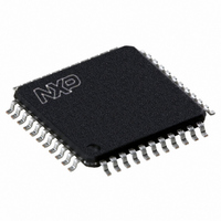
IC 80C51 MCU FLASH 32K 44-TQFP
Manufacturer
NXP Semiconductors
Series
89Vr
Datasheet
1.P89V660FBC557.pdf
(89 pages)
Specifications of P89V662FBC,557
Program Memory Type
FLASH
Program Memory Size
32KB (32K x 8)
Package / Case
44-TQFP
Core Processor
8051
Core Size
8-Bit
Speed
40MHz
Connectivity
I²C, SPI, UART/USART
Peripherals
POR, PWM, WDT
Number Of I /o
36
Ram Size
1K x 8
Voltage - Supply (vcc/vdd)
4.5 V ~ 5.5 V
Oscillator Type
Internal
Operating Temperature
-40°C ~ 85°C
Processor Series
P89V6x
Core
80C51
Data Bus Width
8 bit
Data Ram Size
1 KB
Interface Type
I2C/UART
Maximum Clock Frequency
40 MHz
Number Of Programmable I/os
36
Number Of Timers
3
Operating Supply Voltage
4.5 V to 5.5 V
Maximum Operating Temperature
+ 85 C
Mounting Style
SMD/SMT
3rd Party Development Tools
PK51, CA51, A51, ULINK2
Minimum Operating Temperature
- 40 C
Lead Free Status / RoHS Status
Lead free / RoHS Compliant
For Use With
622-1001 - USB IN-CIRCUIT PROG 80C51ISP
Eeprom Size
-
Data Converters
-
Lead Free Status / Rohs Status
Lead free / RoHS Compliant
Other names
568-2435
935280832557
P89V662FBC
935280832557
P89V662FBC
Available stocks
Company
Part Number
Manufacturer
Quantity
Price
Company:

Part Number:
P89V662FBC,557
Manufacturer:
Maxim
Quantity:
260
Company:
Part Number:
P89V662FBC,557
Manufacturer:
NXP Semiconductors
Quantity:
10 000


NXP Semiconductors
9. Dynamic characteristics
Table 71.
Over operating conditions: load capacitance for Port 0, ALE, and PSEN = 100 pF; load capacitance for all other
outputs = 80 pF
T
[1]
[2]
P89V660_662_664_3
Product data sheet
Symbol Parameter
f
t
t
t
t
t
t
t
t
t
t
t
t
t
t
t
t
t
t
t
t
t
t
t
t
t
osc
LHLL
AVLL
LLAX
LLIV
LLPL
PLPH
PLIV
PXIX
PXIZ
PXAV
AVIV
PLAZ
RLRH
WLWH
RLDV
RHDX
RHDZ
LLDV
AVDV
LLWL
AVWL
WHQX
QVWH
RLAZ
WHLH
amb
T
Calculated values are for 6-clock mode only.
= 40 C to +85 C; V
cy(clk)
oscillator frequency
ALE pulse width
address valid to ALE LOW time
address hold after ALE LOW time
ALE LOW to valid instruction in time
ALE LOW to PSEN LOW time
PSEN pulse width
PSEN LOW to valid instruction in
time
input instruction hold after PSEN time
input instruction float after PSEN time
PSEN to address valid time
address to valid instruction in time
PSEN LOW to address float time
RD LOW pulse width
WR LOW pulse width
RD LOW to valid data in time
data hold after RD time
data float after RD time
ALE LOW to valid data in time
address to valid data in time
ALE LOW to RD or WR LOW time
address to RD or WR LOW time
data hold after WR time
data output valid to WR HIGH time
RD LOW to address float time
RD or WR HIGH to ALE HIGH time
= 1 / f
Dynamic characteristics
osc
.
DD
= 4.5 V to 5.5 V; V
Rev. 03 — 10 November 2008
SS
Conditions
12-clock mode
6-clock mode
IAP
= 0 V
[1][2]
80C51 with 512 B/1 kB/2 kB RAM, dual I
Min
0
0
0.25
2T
T
T
-
T
3T
-
0
-
T
-
-
6T
6T
-
0
-
-
-
3T
4T
T
7T
-
T
cy(clk)
cy(clk)
cy(clk)
cy(clk)
cy(clk)
cy(clk)
cy(clk)
cy(clk)
cy(clk)
cy(clk)
cy(clk)
cy(clk)
cy(clk)
P89V660/662/664
15
15
15
8
20
15
15
15
30
30
15
30
50
Typ
-
-
-
-
-
-
-
-
-
-
-
-
-
-
-
-
-
-
-
-
-
-
-
-
-
-
-
-
Max
40
20
40
-
-
-
4T
-
-
3T
-
T
-
5T
10
-
-
5T
-
2T
8T
9T
3T
-
-
-
0
T
cy(clk)
cy(clk)
cy(clk)
cy(clk)
cy(clk)
cy(clk)
cy(clk)
cy(clk)
cy(clk)
cy(clk)
© NXP B.V. 2008. All rights reserved.
+ 15
+ 15
15
2
45
50
60
50
12
50
75
C-bus, SPI
Unit
MHz
MHz
MHz
ns
ns
ns
ns
ns
ns
ns
ns
ns
ns
ns
ns
ns
ns
ns
ns
ns
ns
ns
ns
ns
ns
ns
ns
ns
74 of 89
Related parts for P89V662FBC,557
Image
Part Number
Description
Manufacturer
Datasheet
Request
R

Part Number:
Description:
NXP Semiconductors designed the LPC2420/2460 microcontroller around a 16-bit/32-bitARM7TDMI-S CPU core with real-time debug interfaces that include both JTAG andembedded trace
Manufacturer:
NXP Semiconductors
Datasheet:

Part Number:
Description:
NXP Semiconductors designed the LPC2458 microcontroller around a 16-bit/32-bitARM7TDMI-S CPU core with real-time debug interfaces that include both JTAG andembedded trace
Manufacturer:
NXP Semiconductors
Datasheet:
Part Number:
Description:
NXP Semiconductors designed the LPC2468 microcontroller around a 16-bit/32-bitARM7TDMI-S CPU core with real-time debug interfaces that include both JTAG andembedded trace
Manufacturer:
NXP Semiconductors
Datasheet:
Part Number:
Description:
NXP Semiconductors designed the LPC2470 microcontroller, powered by theARM7TDMI-S core, to be a highly integrated microcontroller for a wide range ofapplications that require advanced communications and high quality graphic displays
Manufacturer:
NXP Semiconductors
Datasheet:
Part Number:
Description:
NXP Semiconductors designed the LPC2478 microcontroller, powered by theARM7TDMI-S core, to be a highly integrated microcontroller for a wide range ofapplications that require advanced communications and high quality graphic displays
Manufacturer:
NXP Semiconductors
Datasheet:
Part Number:
Description:
The Philips Semiconductors XA (eXtended Architecture) family of 16-bit single-chip microcontrollers is powerful enough to easily handle the requirements of high performance embedded applications, yet inexpensive enough to compete in the market for hi
Manufacturer:
NXP Semiconductors
Datasheet:
Part Number:
Description:
The XA-S3 device is a member of Philips Semiconductors? XA(eXtended Architecture) family of high performance 16-bitsingle-chip microcontrollers
Manufacturer:
NXP Semiconductors
Datasheet:

Part Number:
Description:
The NXP BlueStreak LH75401/LH75411 family consists of two low-cost 16/32-bit System-on-Chip (SoC) devices
Manufacturer:
NXP Semiconductors
Datasheet:
Part Number:
Description:
The NXP LPC3130/3131 combine an 180 MHz ARM926EJ-S CPU core, high-speed USB2
Manufacturer:
NXP Semiconductors
Datasheet:
Part Number:
Description:
The NXP LPC3141 combine a 270 MHz ARM926EJ-S CPU core, High-speed USB 2
Manufacturer:
NXP Semiconductors
Part Number:
Description:
The NXP LPC3143 combine a 270 MHz ARM926EJ-S CPU core, High-speed USB 2
Manufacturer:
NXP Semiconductors

Part Number:
Description:
The NXP LPC3152 combines an 180 MHz ARM926EJ-S CPU core, High-speed USB 2
Manufacturer:
NXP Semiconductors
Part Number:
Description:
The NXP LPC3154 combines an 180 MHz ARM926EJ-S CPU core, High-speed USB 2
Manufacturer:
NXP Semiconductors

Part Number:
Description:
Standard level N-channel enhancement mode Field-Effect Transistor (FET) in a plastic package using NXP High-Performance Automotive (HPA) TrenchMOS technology
Manufacturer:
NXP Semiconductors
Datasheet: